Lab Final Project - design, layout, and simulation of an 8-bit ALU
Authored by Nolan Moore
Date: November 8, 2013
Email: mooren14@unlv.nevada.edu
Project Directions
Project .jelib
Lab 7 .jelib (may be required for project .jelib)
Lab 6 .jelib (may be required for project .jelib)
Stimuli data for IRSIM simulation of ALU
Introduction
For the final project in this class, the labs that we have performed up to this point will culminate in a final device called an ALU or Arithmetic Logic Unit. ALUs perform arithmetic functions, such as addition or subtraction, and logical operations, such as AND and OR. The ALU that we will design for this project will utilize all 4 of these operations. Additionally, the ALU will operate on 8-bit inputs and outputs.
The inputs will consist of two 8-bit signals A and B that will be the operands and a 2-bit signal F used to determine which of the 4 operations will be performed. The output will be another 8-bit signal Z. Previously in Lab 7, we created 8-bit versions of each of the logic gates and full adders used in the ALU, and we will be utilizing these previous designs to complete our project.
Seen below is the schematic of thr ALU. The inputs A and B are directly connected to the AND and OR gates, but only A is directly connected to the full adder. B and its inverse B`are connected to a 2-1 MUX that is switched depending on whether addition or subtraction is used. The output of this MUX then goes into the full adder. Another MUX determines whether AND or OR will be used, and the final output is determined by another MUX to be either one of the logical operations or the arithmetic operations. F[0] is used to determine whether AND or OR is used and also whether addition or subtraction is used. F[1] determines the final output.
Complete 8-bit ALU Schematic

Truth table of F[1:0] illustrating functions performed

Arithmetic Operations (F[1] = 0)
Addition (F[0] = 0)
For the addition function, we will use the 8-bit full adder designed in Lab 7. As previously mentioned, A is directly connected, and B is chosen from the MUX by F[0] = 0. The carry out bit from the first full adder bit is connected to the second full adder carry in bit (Cout[0] -> Cin[1]), and this trend is repeated for each further bit. The final carry out bit is ignored for this project, and the first carry in bit is connected to F[0], which is 0 during addition. The full adder used in the ALU is clipped and shown to the right for greater clarity.

Subtraction (F[0] = 1)
For subtraction, the full adder is reused. We will use 2s complement subtraction for this project, and as such, A and B` will be inputs. Subtraction is chosen when F[0] = 1, and this bit also feeds into the full adder, providing the first carry in bit for the full adders. The carry out and in bits are connected the same as previously.Logical Operations (F[1] = 1)
OR (F[0] = 0)
The 8-bit OR gate was designed in Lab 7 and will be reused for this project. The OR gate consists of 8 NOR gates each followed by an inverter. A and B both directly feed into the gate, which is chosen by the following MUX when F[0] = 0.
AND (F[0] = 1)
The 8-bit AND gate was designed in Lab 7 and will be reused for this project. The AND gate consists of 8 NAND gates each followed by an inverter. A and B both directly feed into the gate, which is chosen by the following MUX when F[0] = 1.
LTSpice Simulation
For this simulation, we will set A to be 10011101 (0x9D) and B to be 00100111 (0x27). We will test each operation by changing F[1:0] from 0x0 to 0x3.
Simulation Schematic

Simulation Result
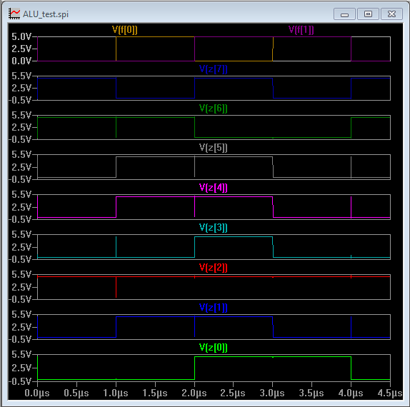
The results are exactly as expected:
Addition: 11000100 (0xC4)
Subtraction: 01110110 (0x76)
OR: 10111111 (0xBF)
AND: 00000101 (0x05)
IRSIM Simulation
For this simulation, we will set A to be 10011101 (0x9D) and B to be 00100111 (0x27). We will test each operation by changing F[1:0] from 0x0 to 0x3.

The results are mostly as expected. The only issue can be seen when F becomes 0x2. Z becomes 0xBF (correct) momentarily before becoming 0x85. After F = 0x3, switching back to F = 0x2 provides the correct result of 0xBF. This problem does not seem to persist when loading the stimuli data.
Addition: 11000100 (0xC4)
Subtraction: 01110110 (0x76)
OR: 10111111 (0xBF)
AND: 00000101 (0x05)
Return Home