Authored by Ruben Medina
E-mail: medina72@unlv.nevada.edu
Date: 10/11/13
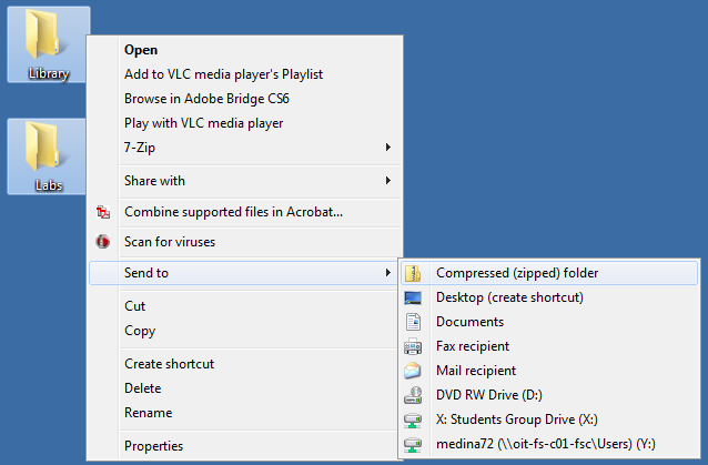
For the pre-lab I first backed up my library and labs by zipping them and uploading the zipped file to Dropbox.

I next went through Tutorial 4 and Electric_video_11 located here.
Then
I read over the lab before starting to work on it.
For the first part of the lab I drafted the schematic and made an icon for a 2-input NAND gate using 10/2 MOSFETs (for both NMOS and PMOS)
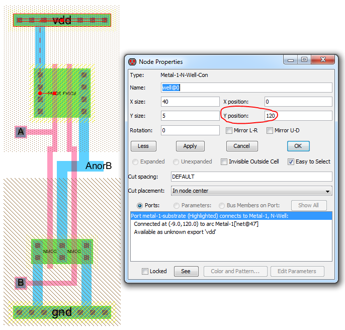
Next, I created a layout for the NAND gate.
For this lab, I chose a standard cell frame (sframe) height of 120λ for all of my gates.
To ensure this height for all of the gate layouts I placed the gnd p-well at the 0,0 position which allowed me to easily move the vdd n-well to my desired height of 120λ. The two PMOS gates can be combined due to having the same source and drain connections.
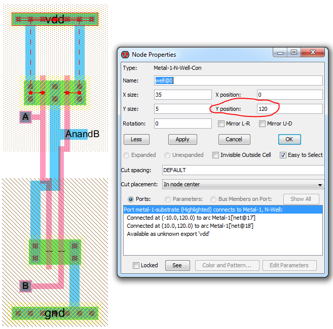
I also added pure n-well and pure p-well nodes to cover more of the appropriate areas of the NAND gate.
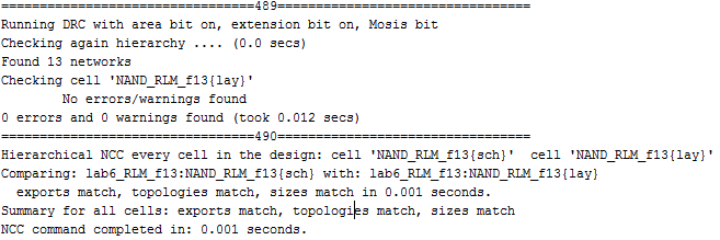
After finishing the layout, I ran DRC (f5) and LVS (l) checks on the layout:
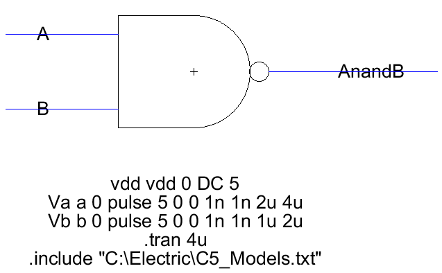
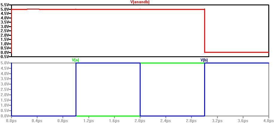
To verify the correct operation of the NAND gate I made a new schematic cell and added the icon of the NAND I created before as well as appropriate net labels and spice code.
I then simulated the NAND gate with LTspice:
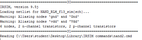
Followed by a simulation of the NAND gate using IRSIM and the command file I made located here by going to Tools -> Simulation (Built-in) -> Restore Stimuli from Disk...:
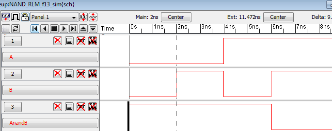
We can see in the error window that the assertions made in the command file for each section of output were all correct (no errors displayed) and the NAND gate is working correctly:
Next, I drafted the schematic and icon for a 2-input NOR gate using 20/2 PMOS and 10/2 NMOS devices.
I then created the layout again using an sframe height of 120λ similar to the NAND gate. For the NOR layout, the two NMOS gates can be combined due to having the same connections of source and drain.
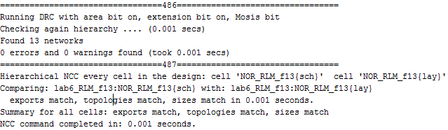
After finishing the layout I ran DRC (f5) and LVS (l) checks on the layout and schematic of the NOR gate:
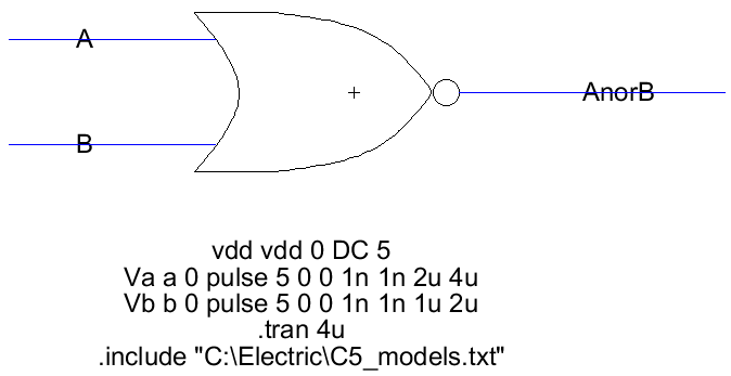
To verify the correct operation of the NOR gate I again created a new schematic with the icon, connections, and spice code.
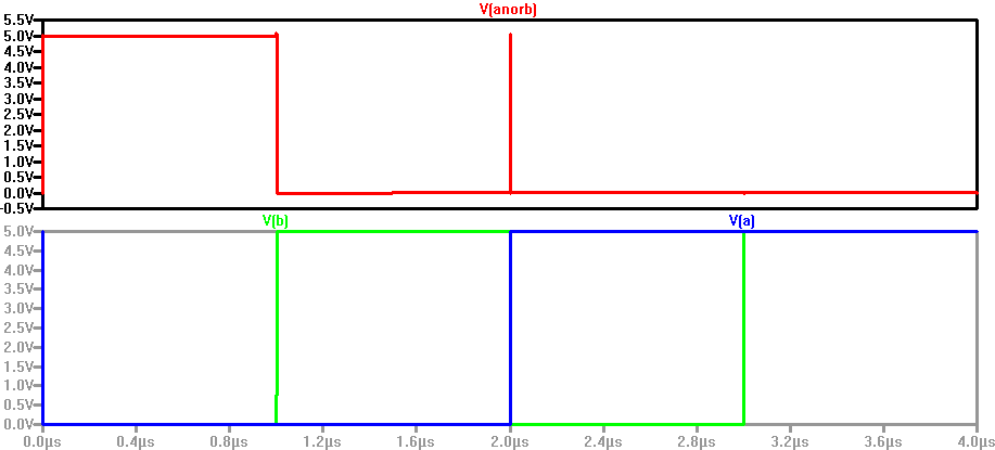
I then simulated the NOR gate with LTspice:
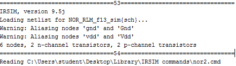
Next, I simulated the NOR gate using IRSIM like was done for the NAND gate using the IRSIM command file located here:
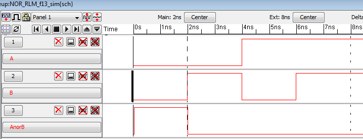
Again we can see in the electric error window that the assertions in the command file match the output signal (no errors) so the NOR is operating correctly.
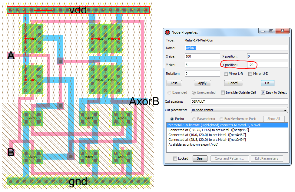
The next gate drafted was a 2-input XOR gate using 20/2 PMOS and 10/2 NMOS devices.
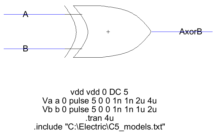
I started again by drafting the schematic and icon for the XOR gate which can be seen below:
I then created the layout for this schematic. To have the A and B inputs be on the same (left) side of the layout I moved the inverter on the right side of the schematic to the left and also separated each inverter so their PMOS and NMOS components were grouped together with the other PMOS and NMOS components in their appropriate wells. Also, because the PMOS devices in the center of the schematic share source and drain connections they were combined in the layout.
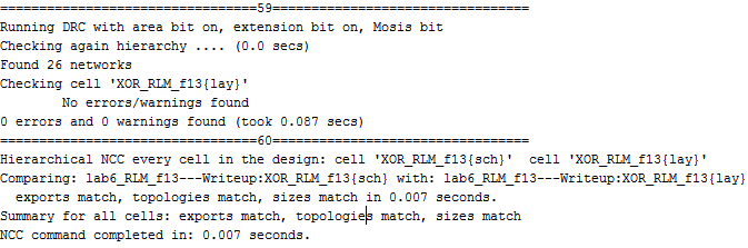
I then ran DRC and LVS checks for the XOR gate:
Next, I created a new schematic and added the XOR icon and spice code to make a simulation cell.
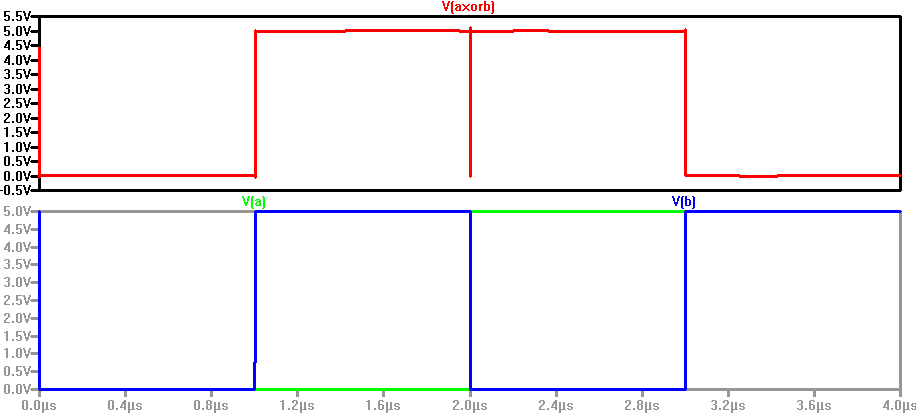
I then simulated the XOR gate using LTspice:
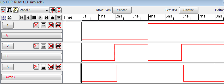
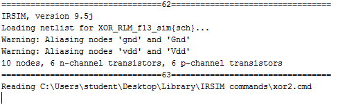
Next, I simulated the XOR gate using IRSIM and the command file located here:
And again we can see from the electric error window that the assertions match the output and the XOR is operating correctly.
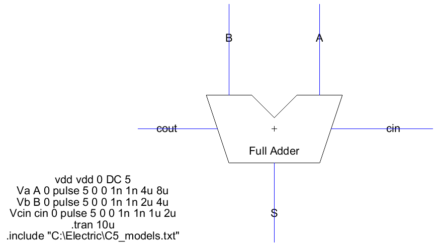
Next, I drafted the schematic of the full adder seen below:

I created the schematic and icon in a new cell:
Then I ran a DRC (f5) on the schematic:
I then made a new schematic cell, added the icon, connections, and spice code:
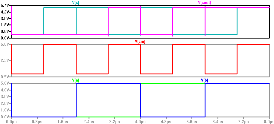
The LTspice simulation of the operation of the full adder:
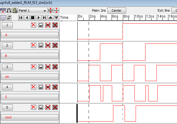
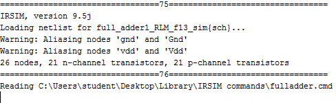
I then ran an IRSIM simulation of the full adder using the command file located here:
Again we can see from the error window that the assertions match the output signals and the full adder is working correctly.
Finally, we needed to show how the full adder seen above could be implemented using 3 NAND gates and 2 XOR gates.
I drafted my schematic and icon as can be seen below:
Then, for the creation of the layout, we were supposed to layout the adder by placing all 5 gates end-to-end so that power and ground are routed which I did and can be seen below:
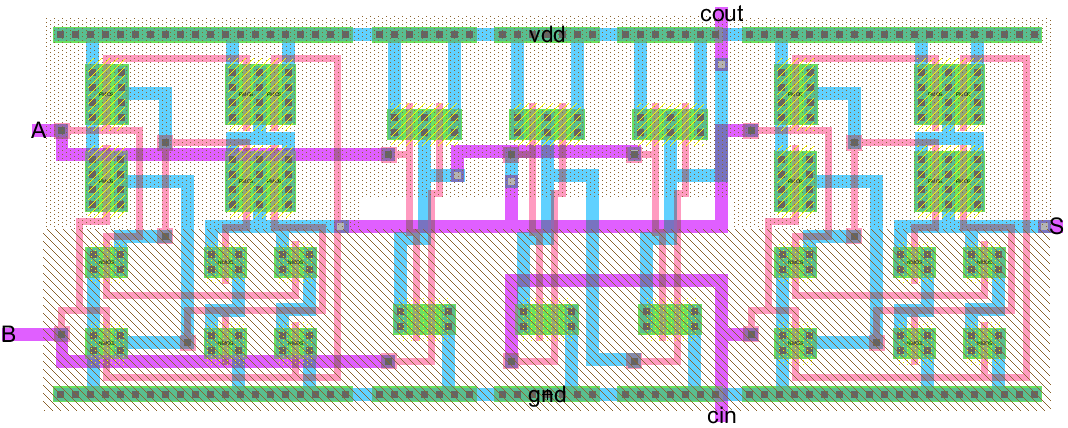
Connections between each gate were done with mostly metal 2 except for a few places where metal 1 use was necessary. Metal 1 was also used to connect the power and ground of each gate and metal 2 was used for the inputs and outputs of the full adder.
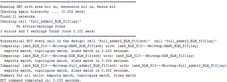
I then ran DRC (f5) and LVS (l) checks on the layout and schematic.
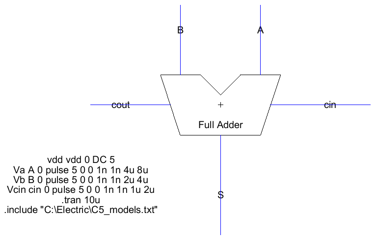
Next up, I created a new schematic cell and added this second adder's icon, connections, and spice code.
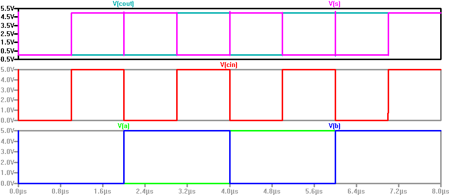
The LTspice results of the simulation can be seen below:
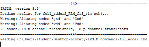
The IRSIM simulation done using the same command file used for the first full adder found here and can be seen below:
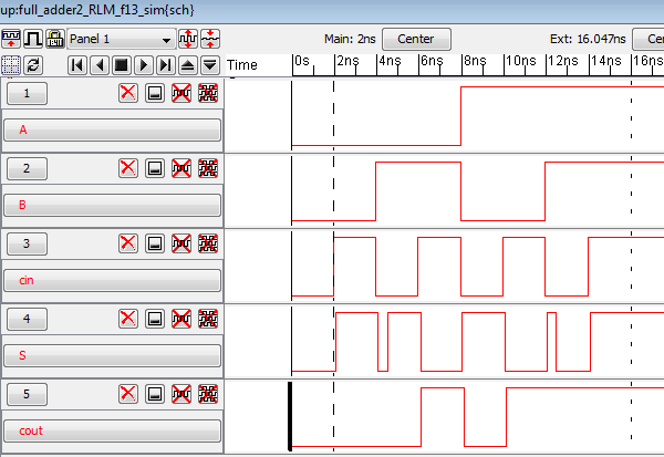
Again we can see in Electric's error window that the assertions match the output signals and the full adder is operating correctly:
My jelib containing the schematics, icons, layouts, and simulation cells for this lab can be found here.
To finish the lab, I zipped my library and lab folder and uploaded the zip file to Dropbox.