Authored by Ruben Medina
E-mail: medina72@unlv.nevada.edu
Date: 10/4/13
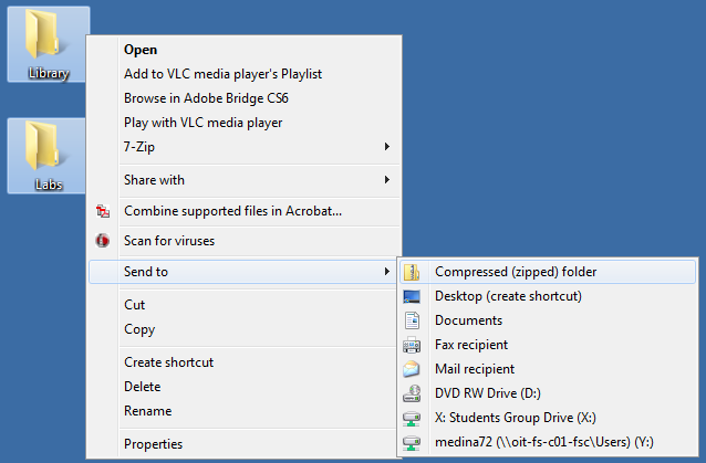
To backup my library and labs I first zipped the folders.
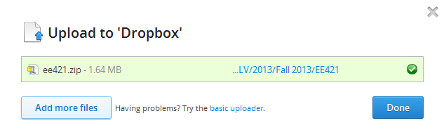
I then uploaded the zipped folder to Dropbox.
I then went through Tutorial 3 located here.
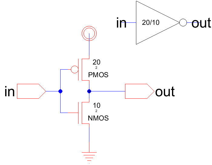
To begin with I started by drafting the schematic and icon for a 20/10 inverter where the 20 is the width of the PMOS and 10 is the width of the NMOS.
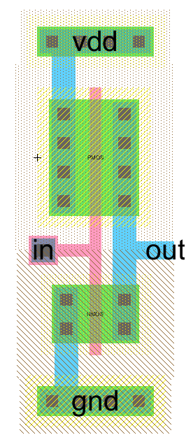
Next, I did the layout for the 20/10 inverter.
Next, I made a schematic for simulation of the inverter with capacitive loads by making a schematic cell and dragging the icon I created into the cell.
I also used off page nodes to export the input and output of the inverter.
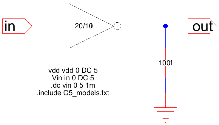
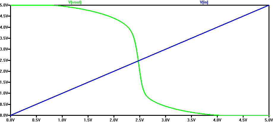
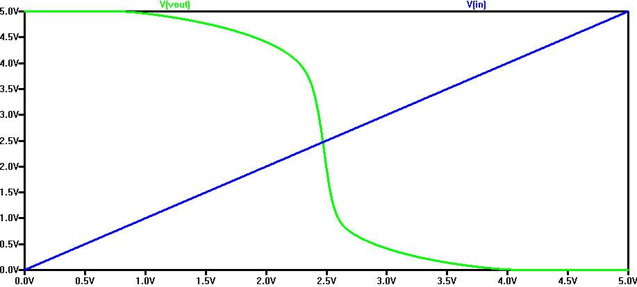
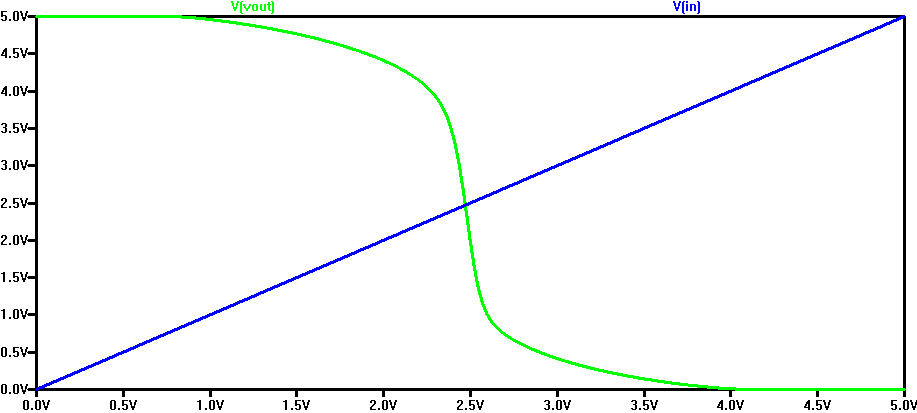
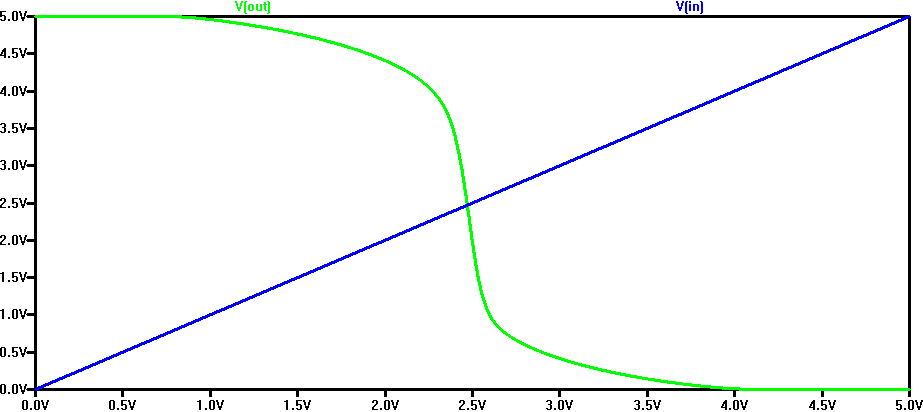
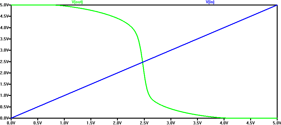
First, I used a capacitive load of 100fF which can be seen above.
The LTspice sim can be seen below:
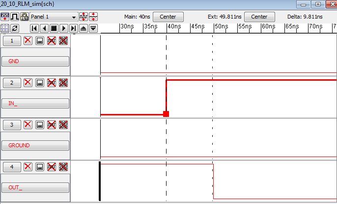
The ALS sim can be seen below:
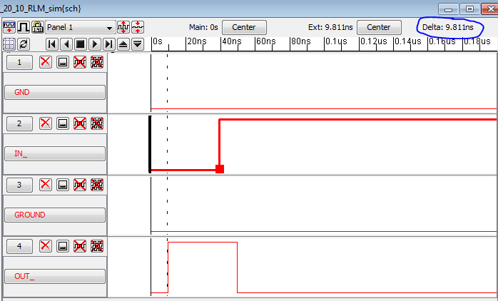
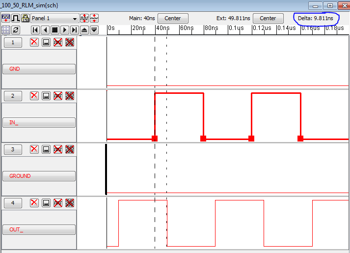
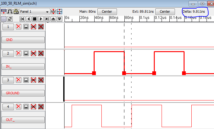
For the ALS simulation, I set the input by moving the cursor to 40ns, then clicked the IN_ button and pressed V to set the waveform high.
I also expanded the waveform size by clicking the button with outward pointing arrows next to "Panel 1".
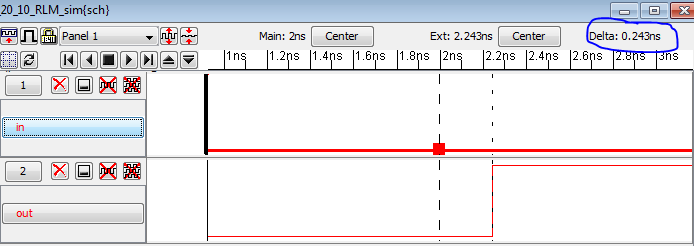
The IRSIM can be seen below:
Next, I ran simulations for a 1pF capacitive load.
The LTspice sim can be seen below:
The ALS sim can be seen below:
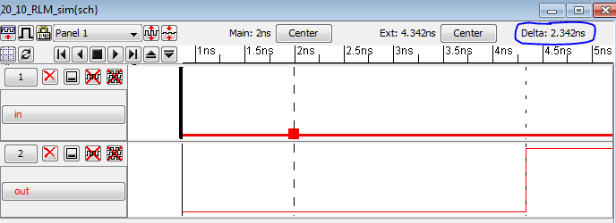
The IRSIM can be seen below:
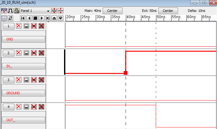
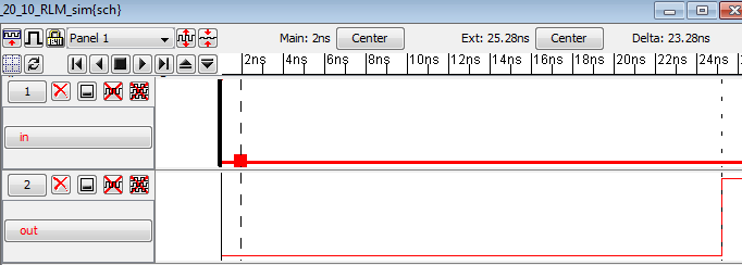
Finally, I ran simulations with a 10pF capacitive load.
The LTspice sim can be seen below:
The ALS sim can be seen below:
The IRSIM can be seen below:
From the simulation results of the various capacitances we can see that the LTspice simulations do not change based on the capacitance due to not taking into account the delay introduced by the capacitors.
We can also see that the delays of all of the ALS simulations were all ~10ns. This is because ALS is a logic simulator and does not model transistors during simulation.
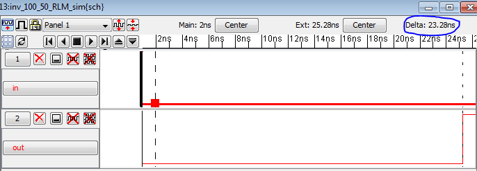
IRSIM on the other hand, does model the transistors and we can see that by the increasing delays of the IRSIM simulations of 0.243ns, 2.342ns, and 23.28ns.
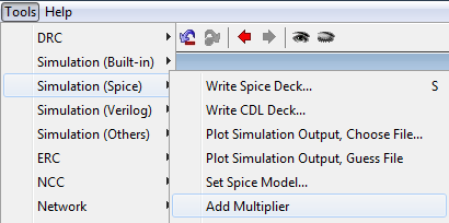
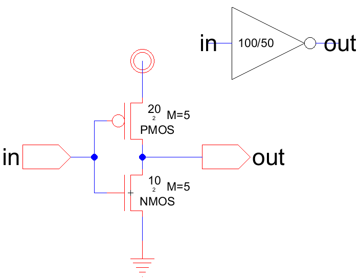
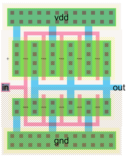
Next, I drafted the schematic and icon for the 100/50 inverter by duplicating the 20/10 inverter cell group and adding a multiplier to the PMOS and NMOS transistors in the schematic.
This was done by going to Tools -> Simulation(Spice) -> Add Multiplier
I then did the layout for the schematic by taking the 20/10 layout, changing the size of the vdd and gnd p-wells and n-wells, copying all of the NMOS and PMOS transistors 4 times, and adding all the required connections.
Next, I made a schematic for the capacitance simulations by making a new cell and dragging the 100/50 icon into the cell.
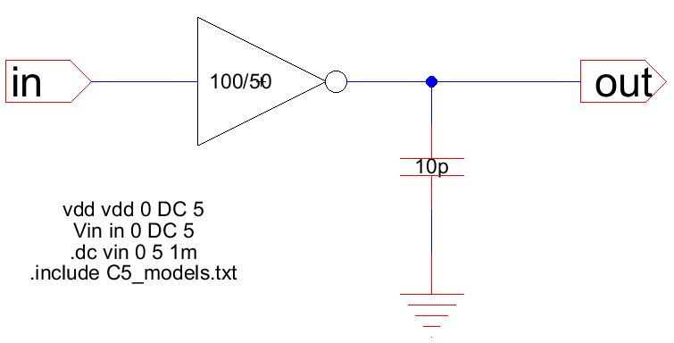
I then ran simulations for the 100f, 1p, and 10p capacitive loads similarly to the 20/10 inverter.
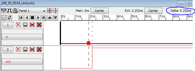
For the 100fF capacitive load:
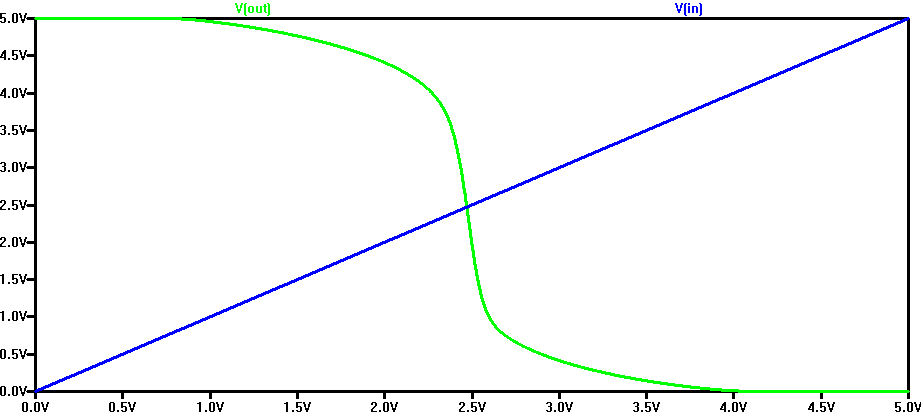
The LTspice sim:
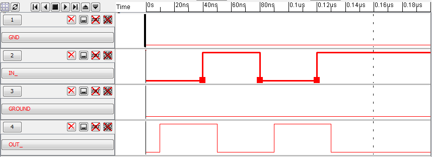
The ALS sim:
The IRSIM simulation:
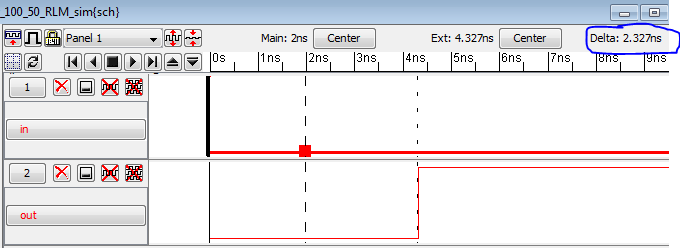
For the 1pF capacitive load:
The LTspice sim:
The ALS simulation:
The IRSIM simulation:
For the 10pF capacitive load:
The LTspice sim:
The ALS simulation:
The IRSIM simulation:
From these simulations we can see again that the LTspice simulations do not change based on capacitance and the delay of the ALS simulations is a constant ~10ns due to not modeling transistors during the simulation.
We can also see that the IRSIM simulations do model the transistors and have an increasing delay based on the increasing capacitance of 0.252ns, 2.327ns, and 23.28ns.
Essentially the simulated delays of the two inverters are the same even though the amount of transistors is different between them.
My electric library file containing my inv_20_10_RLM, inv_20_10_RLM_sim, inv_100_50_RLM, and inv_100_50_RLM_sim can be found here.
To finish the lab I zipped my lab and library folder as seen below:
I then uploaded the zipped file to Dropbox.