Authored by Ruben Medina
E-mail: medina72@unlv.nevada.edu
Date: 9/27/13
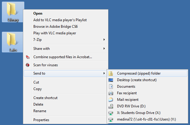
For the first part of the pre-lab I backed up my files by selecting and right clicking the folders and then choosing send to Compressed zip folder
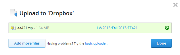
Next, I renamed the zipped folder to ee421.zip and uploaded the folder to Dropbox.
For the second part, I finished Tutorial 2 located here.
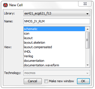
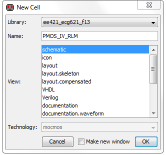
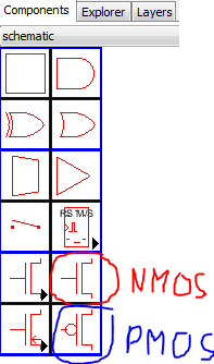
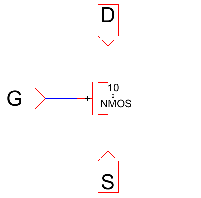
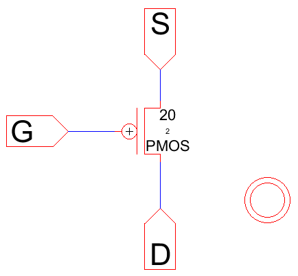
To simulate the IV characteristics of the NMOS and PMOS I first made schematics (ctrl+n or Cell -> New Cell) for each of the MOSFETs.
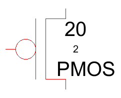
Next, I placed the components for each NMOS and PMOS schematic cell. The width and length for each are 10/2 (3u/0.6u) for NMOS and 20/2 for (6u/0.6u) PMOS.
For each schematic I selected the appropriate MOSFET, NMOS or PMOS.
The width and length was changed by querying (q or ctrl+i) the MOSFET component after it was placed.
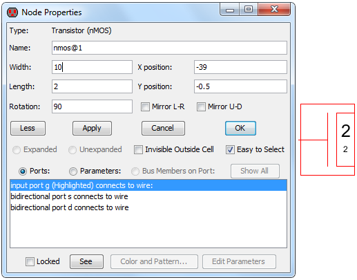
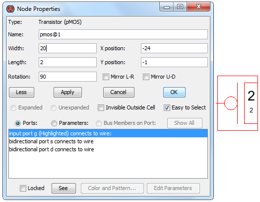
The spice model was set by selecting the MOSFET, going to Tools -> Simulation (Spice) -> Set Spice Model... and then entering NMOS and PMOS for each MOSFET.
Next, I placed off-page nodes for the connections of each MOSFET.
To export the off-page nodes, I selected the node and then pressed ctrl+e and set the appropriate G, D, and S for each MOSFET.
The ground and power nodes are placed in the schematic to match the vdd and gnd components in the layouts for each MOSFET.
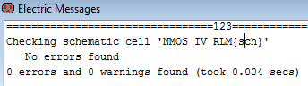
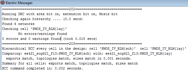
I then ran a DRC error check on each schematic (f5 or Tools -> DRC -> Check Hierarchically).
Next, I made a new cell layout for the NMOS MOSFET.
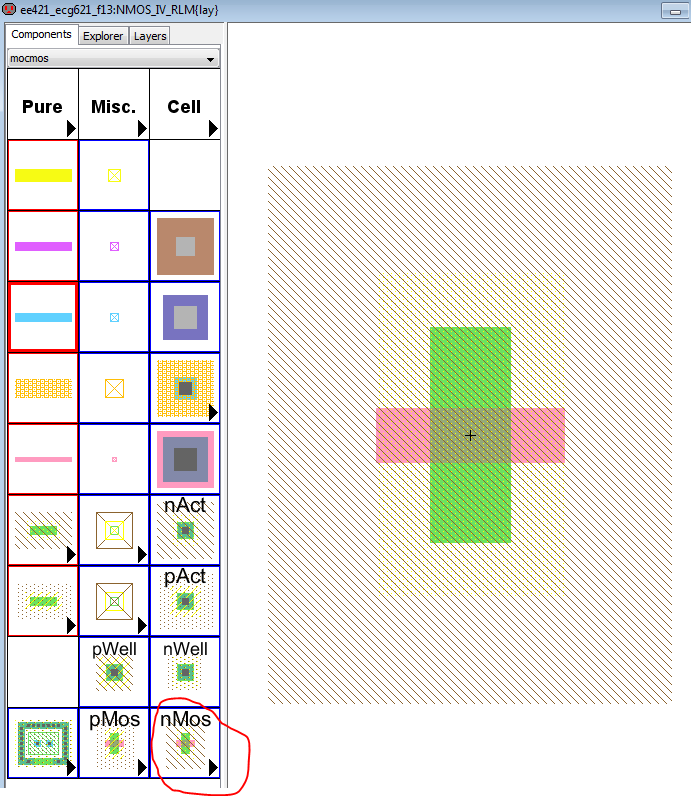
I then changed the size of the NMOS by querying it and changing the width to 10.
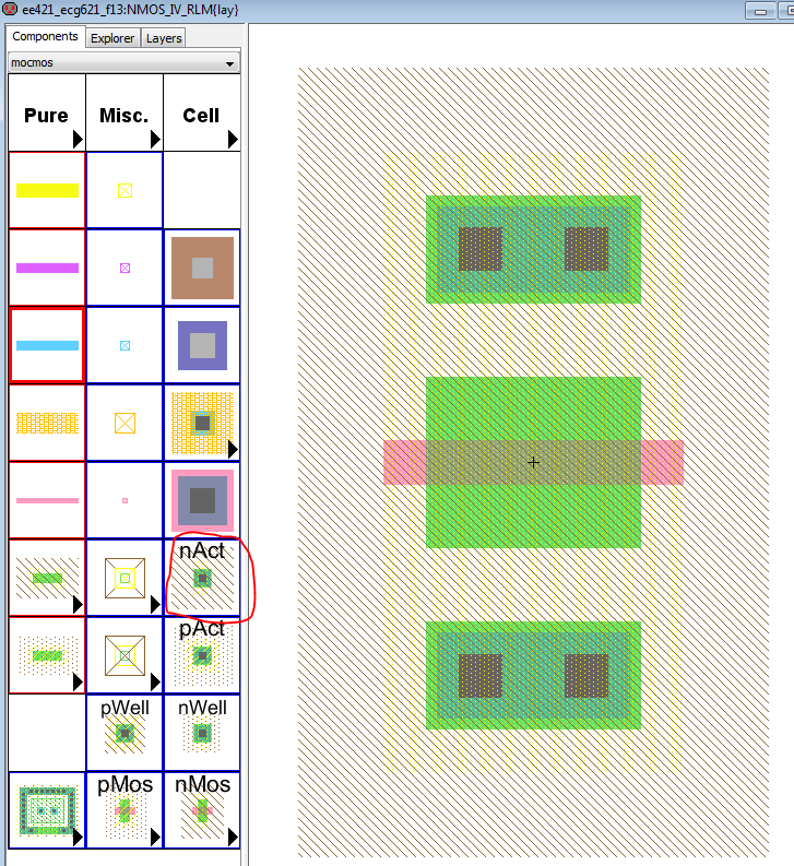
Next I placed two nAct components above and below the NMOS and changed the width of them to 10 by querying them.
Then, I placed a metal one to polysilicon node and a p-well component underneath the NMOS which will be used to connect it to ground.
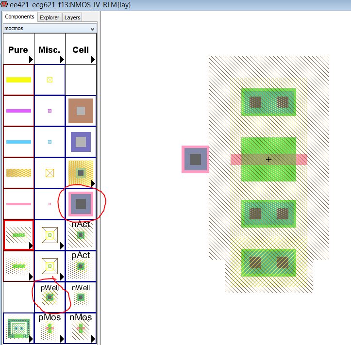
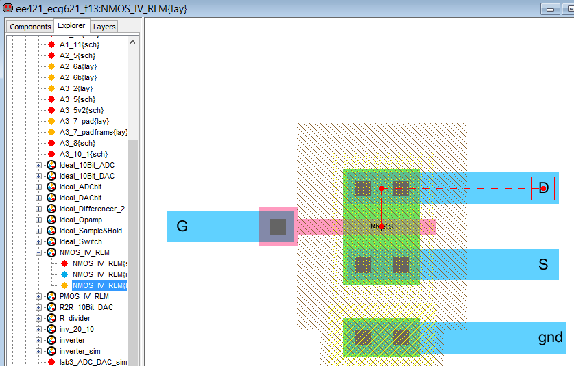
Next, I connected all of the components by clicking each one and right clicking to where I wanted it to be connected. I also added metal one connections for exporting.
I also moved the nAct components closer to the NMOS by clicking on them and using the arrow keys to move them around.
Finally, I added a spice model to the NMOS by selecting the pink gate area and doing it as was done above. Then I added exports to the metal one connections as was done in the schematic.
When adding the exports to the metal one it is important to select the node at the end of the metal one by ctrl-clicking to add the export as can be seen below for the D export.
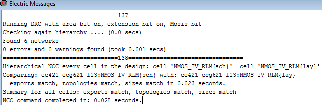
Finally, I ran a DRC and NCC (L or Tools -> NCC -> Schematic and Layout Views of Cell in Current Window) error check on the layout.
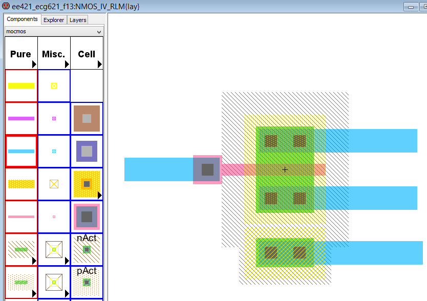
Next I made a layout cell for the PMOS layout and placed components similarly to the NMOS layout.
However, instead of the NMOS component I used the PMOS component and pAct on the top and bottom of the PMOS instead of nAct.
I also changed the width of the PMOS and pAct components to 20 by querying each component.
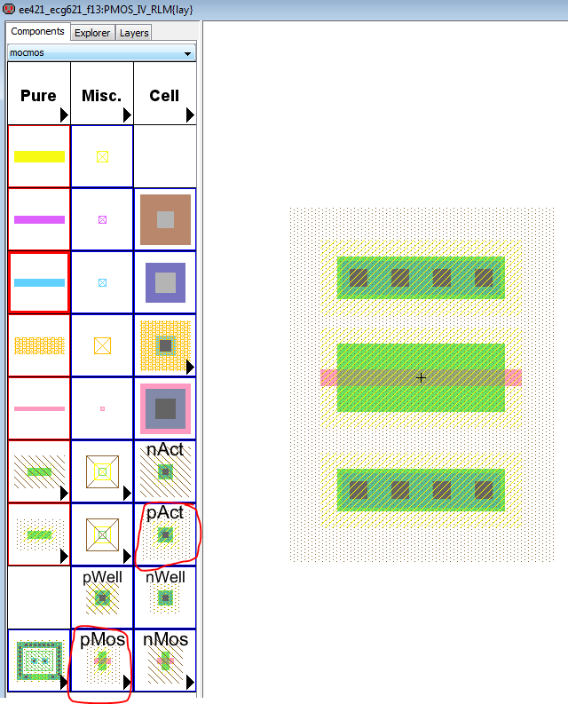
Next I placed a metal one to polysilicon node and an n-well on top of the PMOS for a connection to power.
I also made all of the connections, placed a spice model "PMOS" for the PMOS component, and exported all of the appropriate metal one nodes.
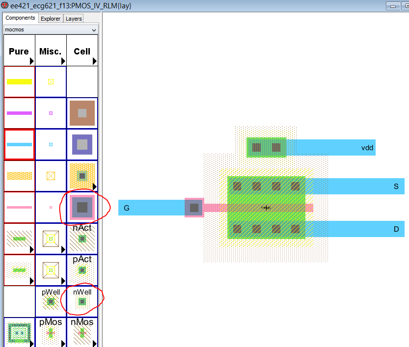
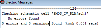
Finally, I ran a DRC and NCC layout check on the PMOS layout.
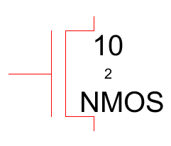
Next, I created icon views of the schematics for each NMOS and PMOS by opening each NMOS and PMOS schematic cell and going to View -> Make Icon View.
The icon views default to a messy box so I deleted the box and made an NMOS using the line tool. I moved the line by selecting it and pressing Y and also added more lines by right clicking. I added text to show the name as well.
I also did the same for the PMOS icon:
I also ran NCC checks for each icon view.
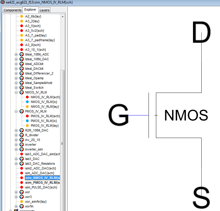
Next, I made new simulation schematic cells for each MOSFET (sim_NMOS_IV_RLM and sim_PMOS_IV_RLM) and dragged the icon cell for each MOSFET into the simulation schematic.
Then I connected wires and sources for each of the simulation schematics and set spice code for the simulation of each of them.
I also labeled the wires by querying them instead of exporting them.
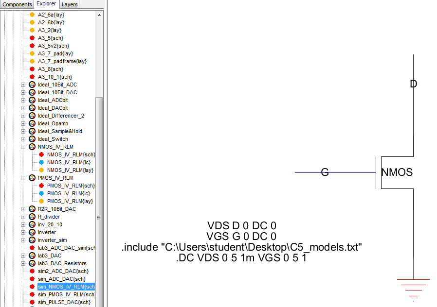
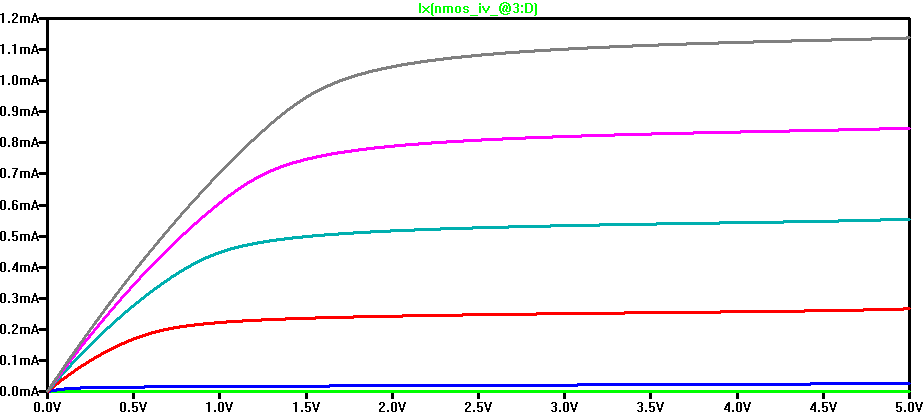
The simulation for the NMOS is given below:
I also did the same for the PMOS simulation schematic.
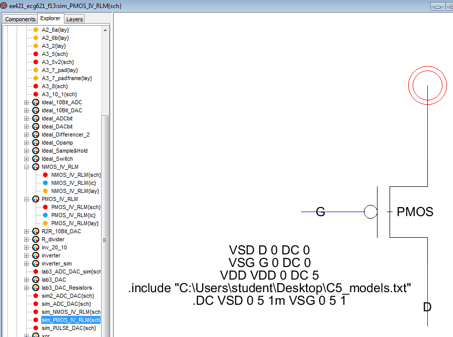
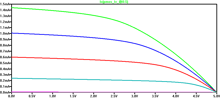
The simulation for the PMOS is given below:
My jelib containing my NMOS_IV_RLM, PMOS_IV_RLM, sim_NMOS_IV_RLM and sim_PMOS_IV_RLM can be found here.
Finally, I backed up my library and labs by zipping them first.
Then I uploaded the zipped file to Dropbox.