In this lab, we will be designing and laying out an inverter from a PMOS and NMOS transistor pair. Prior to this lab, Tutorial 3 should be reviewed.
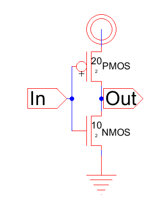
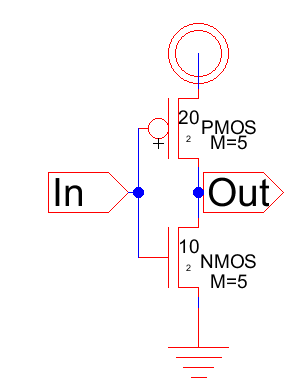
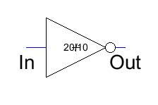
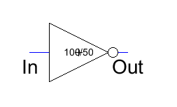
We will have two designs for our work. Our first design is a 10/2 NMOS and a 20/2 PMOS, while our second design includes a multiple of 5, creating an equivalent circuit of 100/2 and 50/2.
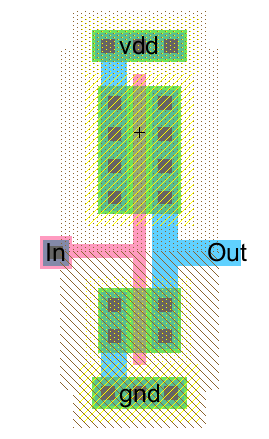
Begin by laying out a PMOS on top and an NMOS on bottom. We can change the model type to 3-terminal by selecting the MOSFET and pressing C. Connect the closer terminals together, and connect the gates. Connect a power source to the top of the PMOS, and a ground at the bottom of the NMOS. Create off-page nodes and export them using Ctrl+E, connecting the In node to the gates and the Out node to the connection between the MOSFETs. The end result should look like the following picture:
Remember to select your MOS devices and set their models to PMOS and NMOS as in the previous lab. Now, duplicate this schematic and in the Tools ->Spice menu, selecing both PMOS and NMOS, create a multiple of 5. The result should be as follows.
Now, we need to create an icon view for both of these, the process will be identical. Go to View -> Make Icon View. Move your In and Out pins and delete the default shape, replacing it with the shape of a standard inverter, placing the schematic information on it. The results should be as follows:
Remember to be clearing pins and running DRC checks as we progress through the experiment.
Now, a layout needs to be created. Create a new layout with the same name as the schematic and icons. Lay out the layout in the same general shape as the schematic. We use NMOS and PMOS for our transistors, Metal1 to Poly for our Gate connections, N-Active for connecting our NMOS Drain and Source to Metal 1, P-Active for connecting our PMOS to Metal 1, an N-well for connecting to VDD, and P-well for connecting to ground. Export In and Out as before, but also export vdd and gnd. The resulting layout is as follows:
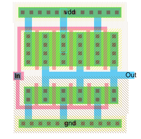
To layout the multiples schematic, simply create multiple transistors and follow the same steps.
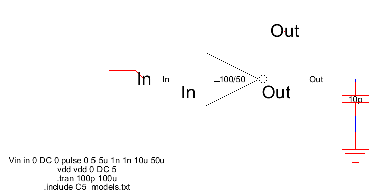
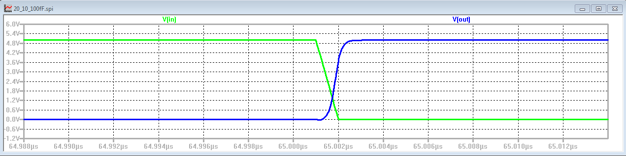
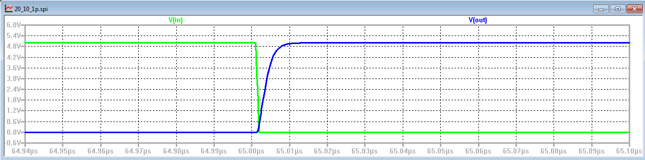
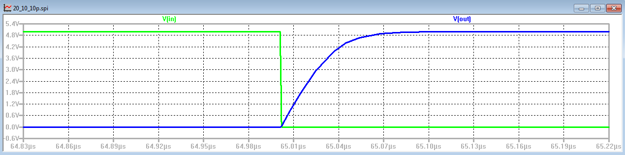
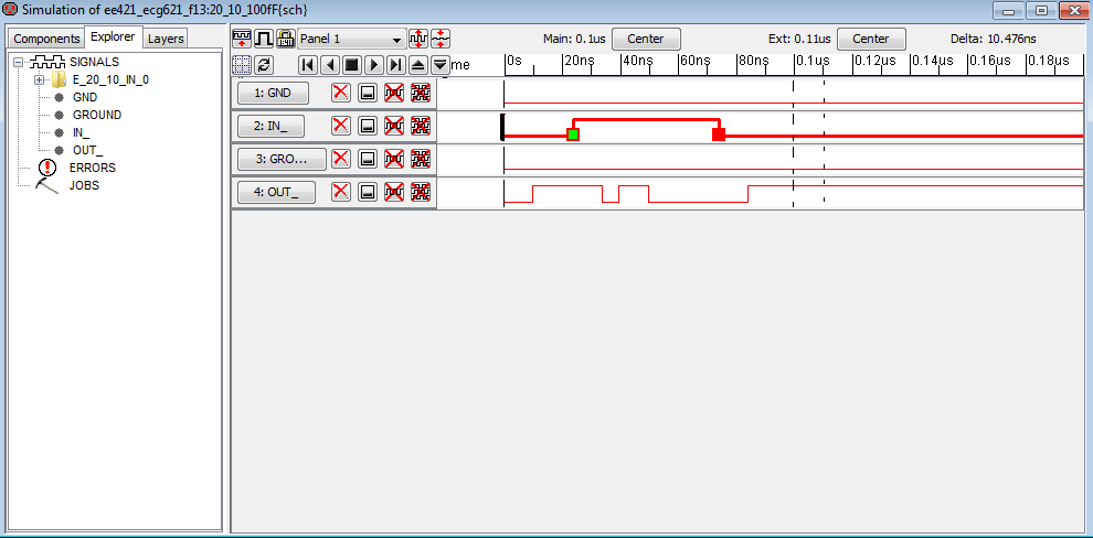
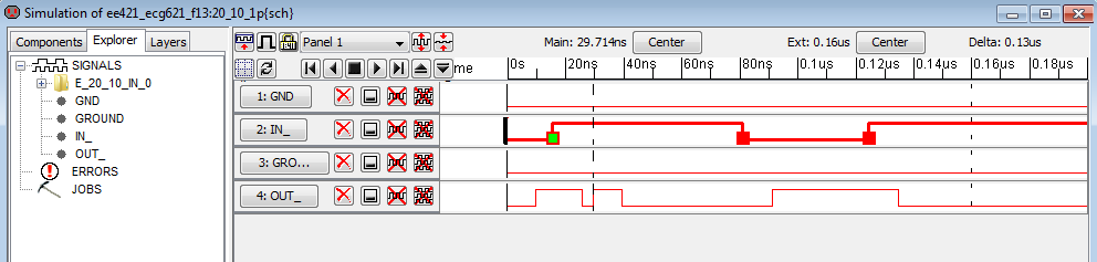
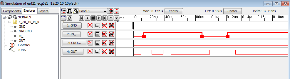
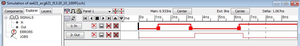
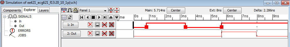
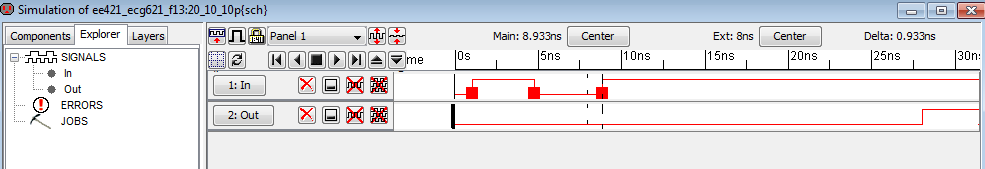
We will be using 3 programs to simulate our results of driving 3 capacitive loads: LTspice, ALS, and IRSIM. Our capacitive loads will be 100fF, 1pF, and 10pF. Our base schematic for the simulations is as follows, and is changed between simulations.