Lab 4 - ECE 421L 

Authored by Stryder Loveday

loveday3@unlv.nevada.edu

September 27, 2013 

In this lab, we will be designing a layout for a PMOS and NMOS transistor.  Before the lab, review Tutorial 2 for Electric VLSI.

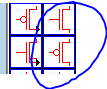
To begin, we shall create two schematic cells, one for NMOS and one for PMOS.  Include initials in the name to verify ownership.

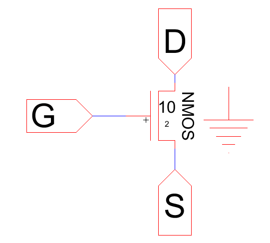
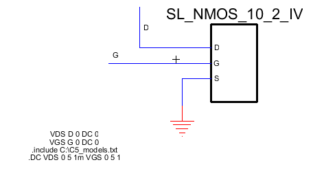
We will begin with the NMOS design.  Select the NMOS transistor from the component list and place it in the schematic.

Components

Download the model file here, and save it to your Electric folder.  It contains model information for devices we will be using.

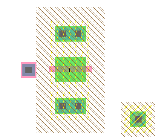
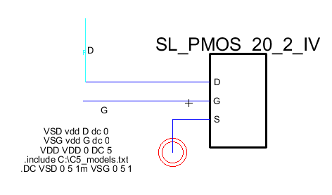
Create an off-page connection for G, S, and D.  Export these off-page connections.  Place a power node for the PMOS, and a ground node for NMOS, to represent the P-Substrate or N-well.  Change the model names to PMOS and NMOS, as is detailed in the text file.  The NMOS sizing is 10/2, while the PMOS sizing is 20/2.  These attributes can be changes by querying the FET devices.

NMOS1
PMOS1

Next, press F5 and perform all required checks to assure the circuit is functioning properly.  Next, create a layout of the PMOS and NMOS with the same name, as was done in the previously reviewed Tutorial 2.  Recall that we will need to also export ground for these layouts as well.

First, lay out the NMOS transistor and adjust the size to 20/2.  

NMOS2

Lay down the N-active wells and resize them as well.  Select the top and bottom portions of the NMOS and connect them to the N-active respectively.
NMOS3


Connect the Polysilicon and metal layers, and export everything.

NMOS4

Construct a similar PMOS device, with appropriate size settings and using vdd in place of gnd.  Remember to use n-active for the n-well connection to VDD.

PMOS4

Now, create an icon using the schematics for the NMOS and PMOS devices.  Go to View -> Create Icon View.  We can customize the icon, but for this lab we have elected to use the default icon with additional text.

NMOS Icon
PMOS Icon

Now, let's run a DC-Sweep simulation for the NMOS and PMOS.  We want to show the diffeences in operation of NMOS and PMOS devices.

NMOS Sim Schematic
NMOS Sim

PMOS Sim Schematic
PMOS Sim

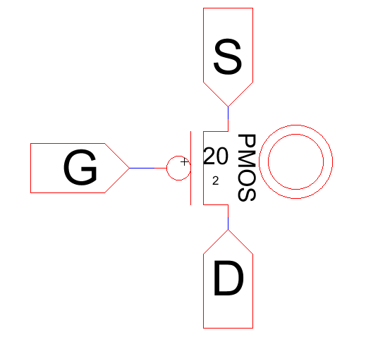
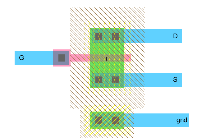
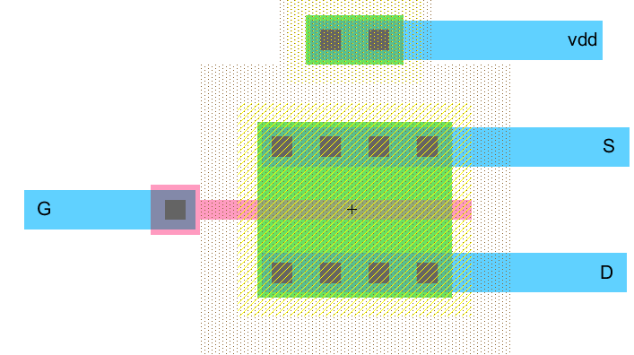
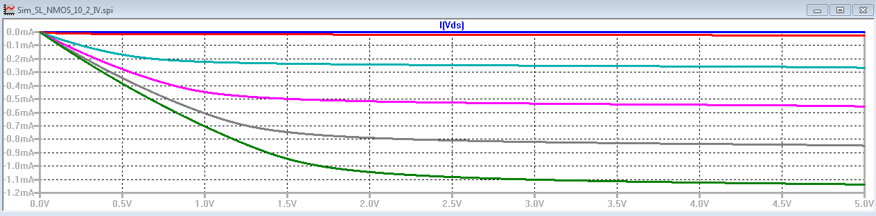
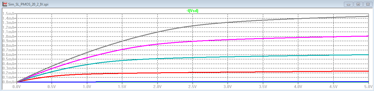
We can see the two MOS devices operate differently, and have different widths to compensate.

A link to my .jelib file is here.

This concludes the Lab 4 report for EE 421.  Please direct any comments or suggestions to Stryder Loveday, at the e-mail address listed above.

Return to EE 421L Labs