Lab 3 - ECE 421L
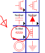
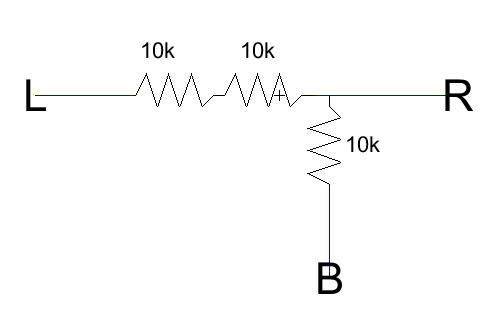
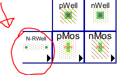
To begin, we will first layout a 10k resistor, using the n-well node, as was discussed in Tutorial one.
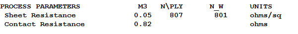
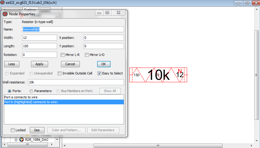
Select the N-well type and place the resistor on the schematic. For this design we want a resistance of 10k. Using MOSIS parameters, we find that the sheet resistance is approximately 801Ω. Using the minimum width of 12 lambda for an N-well, we find that the length required can be determined by 10k = (L/12) * 801. This yields approximately a length of 150 for our resistance of 10k.
Electric measures distances in Lambda, which is the minimum distance MOSIS can handle. For this process, our lambda is 300nm, so our actual width and length for our resistors is 4.5um and 45um respectively.
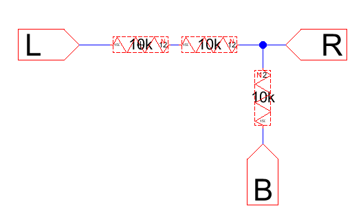
Now that we have an N-well resistor that suits our needs, copy and paste it to have three resistors in the formation previously used for a cell of the DAC constructed in Lab 2.
Create off-page contacts, and export them using Control-E. Next, go to View -> Create Icon View to create a custom icon for this layout. Using the design tools of the icon view, draw a representation of this circuit.
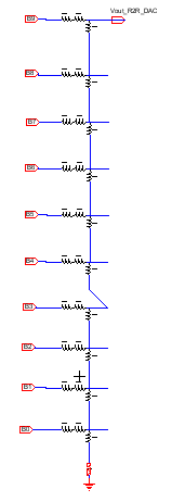
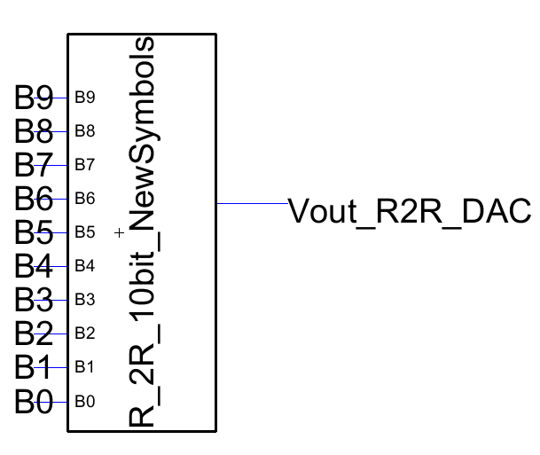
Now that we have a custom-made icon, create ten of these icons on a schematic to recreate the DAC circuit.
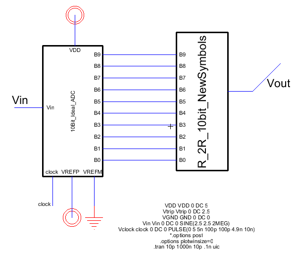
Now that we have our custom circuit, lets create another icon and run the experiment from Lab 2 to test it and verify the icons are functioning properly.
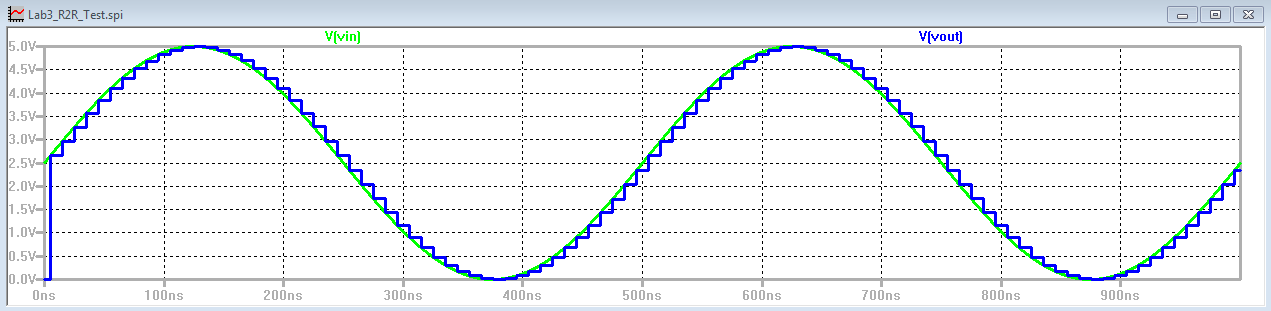
The icons seem to be working well. Now, lets create a layout which will be physically realized in a chip design.
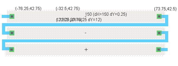
First, create a new layout cell and select N-well resistor. Lay out the resistor, and set the width to 15, and the length to 150.
Lay out 3 resistors stacked vertically, and connect them using Metal 1. This is done by default by selecting the edge connections and right clicking.
Now, lets lay out ten sets of these, to create the entire DAC in layout form. Take caution as to not cross the metal 1 layers, they cannot cross over eachother, other metal layers would need to be used.
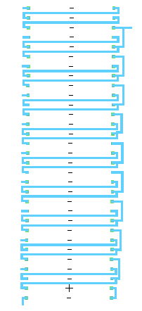
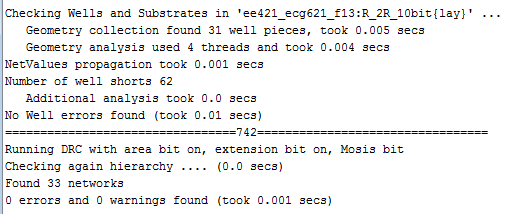
Before we move on, make sure your DRC, NCC, and ERC checks all pass to avoid any future errors.
Next, create a custom icon for this as well, so we can use it in further designs. Export the metal1 nodes used in the positions as the previous DAC design for use in the icon.
![]()
Next, we will test the layout icon in simulation.
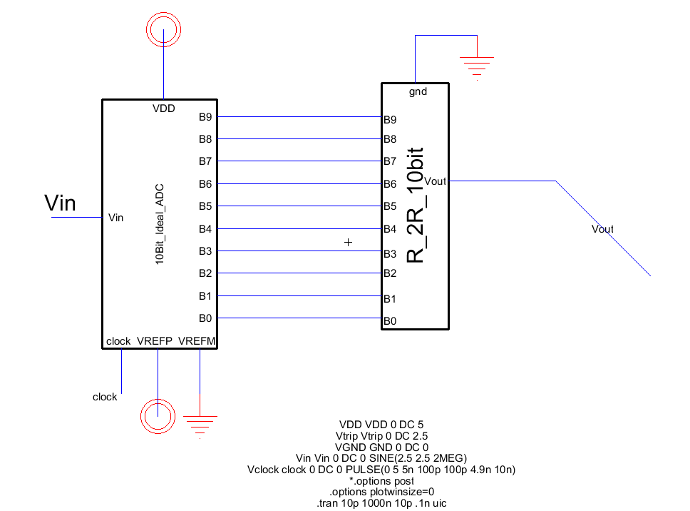
Unfortunately, I was unable to complete this simulation due to an unknown error. This page will be updated when the problem is solved.
As advice to future classes, take the time to organize your filenames and create a system for organization early. Anticipate what you will create and plan accordingly. Issues with integrating previous labs hindered me during this lab, and could have been avoided if proper file names and design trees were used.
Below is a link to my Jelib file. It is a testament to the wrong way to label projects. For this design the cells used were: