Lab 5 - EE 421L
Authored by: Yun Lan
Email: lany3@unlv.nevada.edu
Date: 10/4/13
Lab
description
In
this lab, we will design two CMOS inverters with drawn sizes of 20/10
and 100/50. For 20/10, 20 is the width of the PMOS and 10 is the width
of the NMOS and both MOSFETs have same minumum length of 2. For 100/50,
set M=5 for the 20/2 PMOS and 10/2 NMOS. Draw the schematics, layouts,
and icons for these two inverters. After that, we will run many simulations by using LTspice, ALS, and IRSIM
to verify these inverters.
- 20/10 inverter
- First,
we draw the schematic and make an icon for the 20/10 inverter. The
steps for schematic and icon are straight forward by following Tutorial 3. The off-page nodes are exported as in and out.

- Next,
we will layout the 20/10 inverter. Add one PMOS, two p-actives, one
n-well, one NMOS, two n-acitves, one p-well, one poly1 to metal1
contact, and one metal1 node. Change the width of PMOS and x size
of n-well, p-well, and p-actives to 20. Change the width of NMOS and
x-size of n-actives to 10. Keep the length of these two MOSFETs to the
minimum 2. Connect the actives to MOSFETs and rotate them as seen in
below.

- Connect
the polys of PMOS and NMOS to the p1 to m1 contact and connect the m1
node to the metal 1 in between the NMOS and PMOS. If the size of poly
from the contact to the intersection is too large, you can change the
size to 2.

- Connect vdd
to the PMOS and gnd to the NMOS. Don't forget to export the vdd, gnd,
in, and out, also to set the spice model for PMOS and NMOS.

- Change the text size to 5.

- Here is the final layout for the 20/10 inverter:

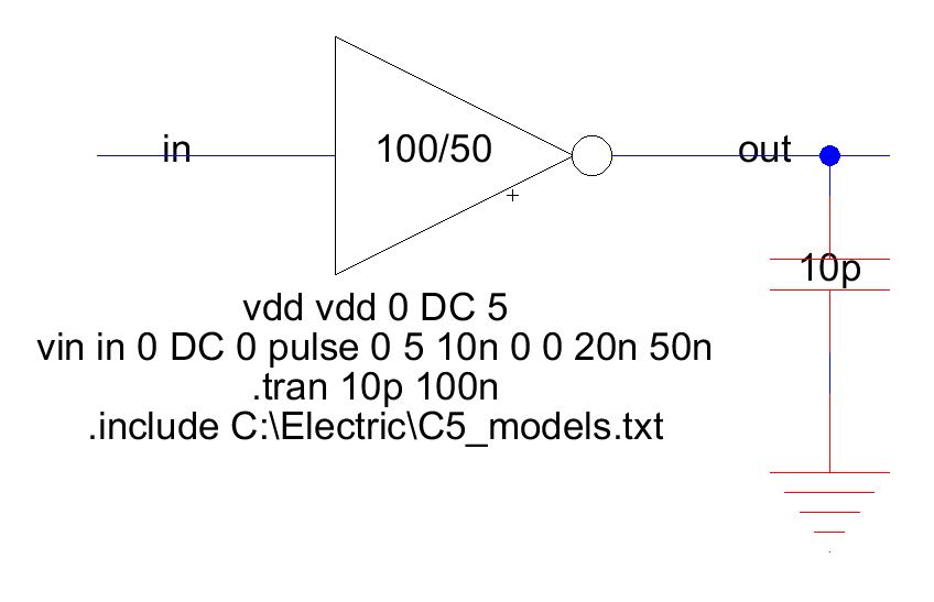
- Now,
let's make a new schematic for simulation. Drag the icon of the
inverter into this schematic and add the spice code as seen below.


- I
also made a layout for simulation. Include the layout of 20/10 inverter
and connect the four nodes to vdd, gnd, in, and out. Note that vdd and
gnd are exports while in and out are the names of the arcs. Copy the
spice code from the schematic.

- Simulate the layout and the simulation is same as the simulation for the schematic.

- Of course, before the simulations, I did DRC, NCC, and ERC.

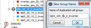
- To start designing the 100/50 inverter, I duplicate the 20/10 inverter and modify them.
- In the schematic, add multipliers for the PMOS and NMOS and set M = 5.


- Add a text to the icon and enter "100/50" to distinguish the 20/10 and 100/50 inverters.

- Next,
modify the layout for the 100/50 inverter. Make five copies of the PMOS
and NMOS, six copies of the p-acitve and n-active, and change the size
of n-well and p-well to align the MOSFETs. Connect the actives to
the MOSFETs and rearrange the positions to make the layout look pretty.
Connect all polys to the poly1 to metal1 contact, PMOS to vdd (n-well),
NMOS to gnd (p-well), and the metal1 in between the MOSFETs to the
metal1 node.

- Here is the final layout for 100/50 inverter:

- Next,
let's simulate the 100/50 inverter. Make a schematic and a layout for
simulation. The steps are same as what I did for the simulations of
20/10 inverter.


- 100/50 inverter simulation result is same as the simulation of 20/10 inverter.

- DRC, NCC, and ERC results:

- SPICE simulations with a capacitor load
- Make a copy of the simulation schematic and modify the spice code and add a 100fF capacitor.

- Simulation with a 100fF capacitor load:

- Simulation with a 1pF capacitor load:

- Simulation
with a 10pF capacitor load. From these three simulations, we can see
that the rise time and fall time of the output changes. Furthermore,
when driving the 10pF capacitor, the peak to peak voltage is from 5V to
about 2.5V, not 5V to 0V.

- Do the same steps for 20/10 inverter to modify the schematic.
- Simulation with a 100fF capacitor load:

- Simulation with a 1pF capacitor load:

- Simulation
with a 10pF capacitor load. Compare to the simulations for 20/10
inverter, we can see that the effect to the 100/50 inverter output rise
and fall time is significantly smaller than the effect in 20/10
inverter.

- ALS simulations for the 20/10 and 100/50 inverters
- Duplicate
the simulation schematic for the 20/10 inverter and modify this
schematic. Delete
the spice code and place both inverters in the schematic as shown
below. Export one input "in" and two outputs "out_20_10" forthe 20/10
inverter output and "out_100_50" for the 100/50 inverter output.

- Click the "ALS: Simulate Current Cell"
from the menu below to do a ALS simulation. Then select the signal "in"
and click "Set Clock on Selected Signal..." as shown below and set the
period or frequency of the clock.


- The
in signal now behaves like a clock. The simulation for 100fF
capacitor load shows that there are delays between the input and
outputs, but the delays for these two outputs are same.

- Simulation with 1pF capacitor load:

- Simulation
with 10pF capacitor load. The delays of the outputs with different load
capacitances are the same. The reason why the delays are same is
because ALS stands for "Asynchronous Logic Simulator". Asynchronous
logic simulation is equivalent to cycle simulation and cycle simulation
runs at a constant speed, regardless of activity in the model (Cited
from Wikipedia: Logic Simulation). Therefore, the capacitor will not
change the delay of the inverter in ALS simulation.

- Finally, simulate the inverters using IRSIM.
- Duplicate the whole group of the ALS simulation schematics. The schematics for IRSIM are exactly same as the schematics for ALS.

- The
IRSIM does not support the clock input, therefore I have to draw the
input myself by clicking Set high and low from the menu: Tools ->
Simation (Built-in) -> Set Signal High (Low) at Main Time.

- Unlike
the ALS, the IRSIM shows the delay of the outputs. The simulation with
100fF capacitor shows the delay of the output of the 20/10
inverter.

- With a larger capacitor, the delay of the output of the 20/10 inverter increases.

- When
the 20/10 inverter is driving a 10pF capacitor, the delay is too large
and the output does not even show anything. We can see that the 100/50
inverter can handle a larger capacitor than the 20/10 inverter. The
simulation does not show any delay for the output of the 100/50
inverter.


Return to lany3/
Return to EE 421L Labs