First we grap our regular 1 bit inverter. Next rename the invert to inverter[7:0] this command implies we now have an array of 8 inverters

Next add buses to the inverter and name the buses in[7:0] and out [7:0] Now we have an array of 8 inverters with 8 inputs and outputs
Finally build an icon

Here is the the icon and the simulation to show the 8bit outputs

Simulation of Vin versus the all 8bit outputs

Here we will test the ouptus with a few capacitors.

Sim results shows that the largest capacitor switchs the slowest as expected.

\
Here I designed a 8bit AND, NAND, NOR, OR , and Inverter.

Here is the AND and NAND sims. Notice the output signals are inverse as expected.

Here is the OR and NOR sims. Notice the output signals are inverse as expected.

Next we will make a DMUX gate.
Here is the Icon and Sim. We can see when "Vs" is low the output fallows "Va" and when low the output fallows "Vb".

The IRSIM results match.

Here is 8bit DEMUX

The 8bit Sims fallows the same results as above.

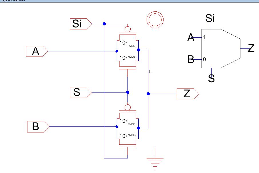
Demux with Z input

Sims


Next we will make a 1 bit full adder
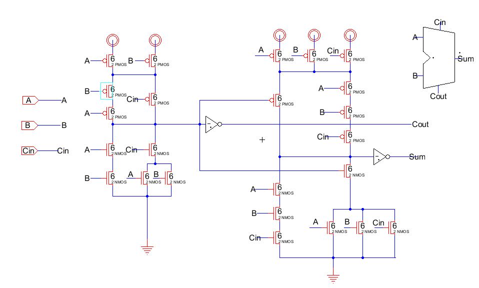
Full adder layout


Here is the sim and works as expected

Here we make an 8bit adder

The 8bit Adder layout

8bit Adder NCC, DRC, and Well check all pass.
 N
N
8bit icon and sim.

A inputs

B inputs

Outputs as expected

