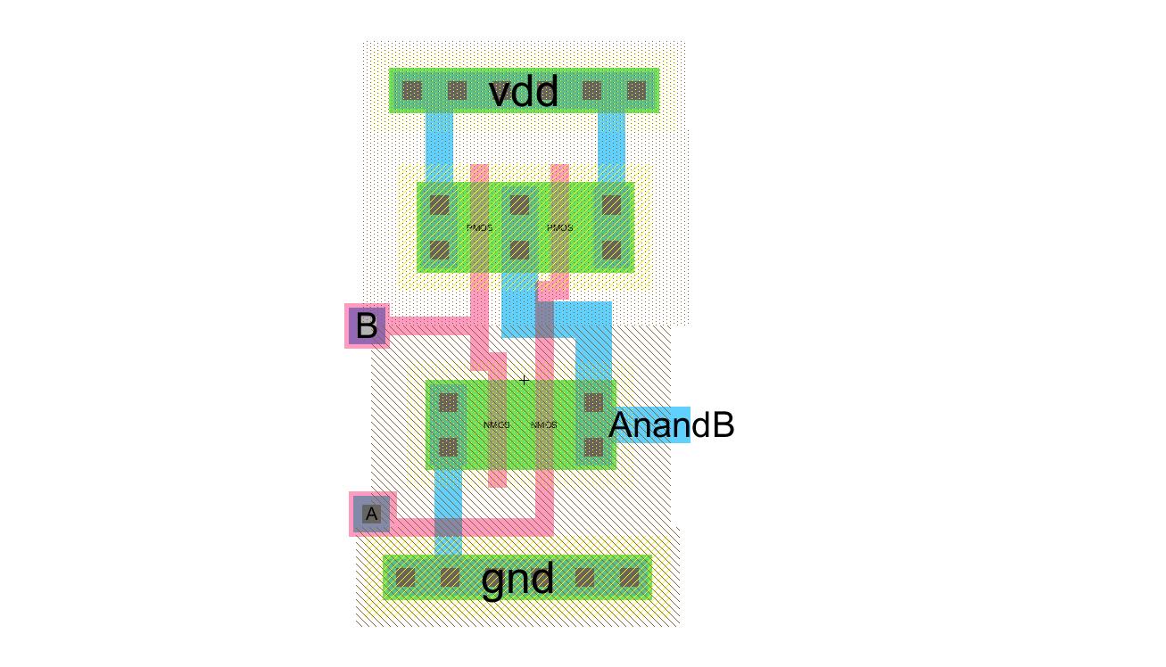
- Draft the schematic of a 2-input NAND gate (Fig. 12.1) using 10/2 MOSFETs (both NMOS and PMOS)

- Create layout and icon views for this gate showing that the cells NCC, DRC, and well-check without errors
- Icon is in the top picture in the top left corner
- Well, NCC, and DRC check fine.

- 3d view

- Using both LTspice and IRSIM simulate the logical operation of the gate for all 4 possible inputs

- NAND truth table

- LTspice Sim


- Repeat these steps for a 2-input NOR gate using 20/2 PMOS devices and 10/2 NMOS devices
- Create an icon for this full-adder


- Simulation


- LTspice Sim.


- Again, repeat these steps for a 2-input XOR gate (Fig. 12.18) noting that the gate will also need two inverters
- For all 12 transistors used in the XOR gate use 20/2 PMOS and 10/2 NMOS devices


- Simulation


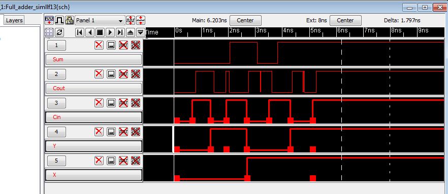
- Using these gates (and 3 inverters), draft the schematic of the full adder seen below
- Create an icon for this full-adder

- Simulate, using LTspice and IRSIM, the operation of the full-adder using this icon


- Show how a full-adder can be implemented using 3 NAND gates and 2 XOR gates

- Layout the full-adder by placing the 5 gates end-to-end so that power and ground are routed
- full-adder inputs and outputs can be on metal2 but not metal3


- NCC, DRC, and well-check your full-adder layout

- Create another icon view and again simulate using LTspice and IRSIM


Backup LAB
