
Lab 5 - EE 421L
October 5, 2013
lamorea3@unlv.nevada.edu
20/10 PMOS/NMOS inverter schematic. Take note of the icon in the top left corner of the picture below.
Layout View of 20/10 PMOS/NMOS inverter. Take note of the 4 pins I exported in, out, gnd, and vdd

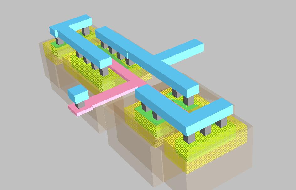
3D View of the PMOS/NMOS inverter
NCC, Well check, and DRC the design.


Simulation of the 20/10 inverter driving 3 capacitive loads 1p, 10p, 100f

We notice in LT Spice that there switch behavior is close to the same. Althoug if i cylced the imputs the 10p capacitor would have the largest lag.
Schmatic of a 20/10 PMOS/NMOS inverter with a multiplyer of 5

Notice the difference in the layout schmatics. This Transistor layout has a 5 multiplier which mean that we have 5 20/10 transistors in parrallel. This also has the same exports as before, in, out, gnd, and vdd

Here is the Well Check, DRC, and NCC of the design

Just as before we simed the inverter with the same capacitive load


