
Lab 4 - EE 421L
September 27, 2013
lamorea3@unlv.nevada.edu
Making the NMOS and PMOS Schematics. Note that I will show the specifics for the NMOS. The PMOS is made in the same way except some minor changes that I will document later.
First grob the NMOS transister, 3 Pins, and gnd.
Next change the size of the NMOS to 10/2 and add exports to the NMOS pins.

Last is we need to add a model name so we can simulate the transister. When the screen pops up label it NMOS.

Next we will create a icon for the NMOS.

You can edit the icon to any custom image you would like.

Last we need to do a DRC check

THE PMOS:
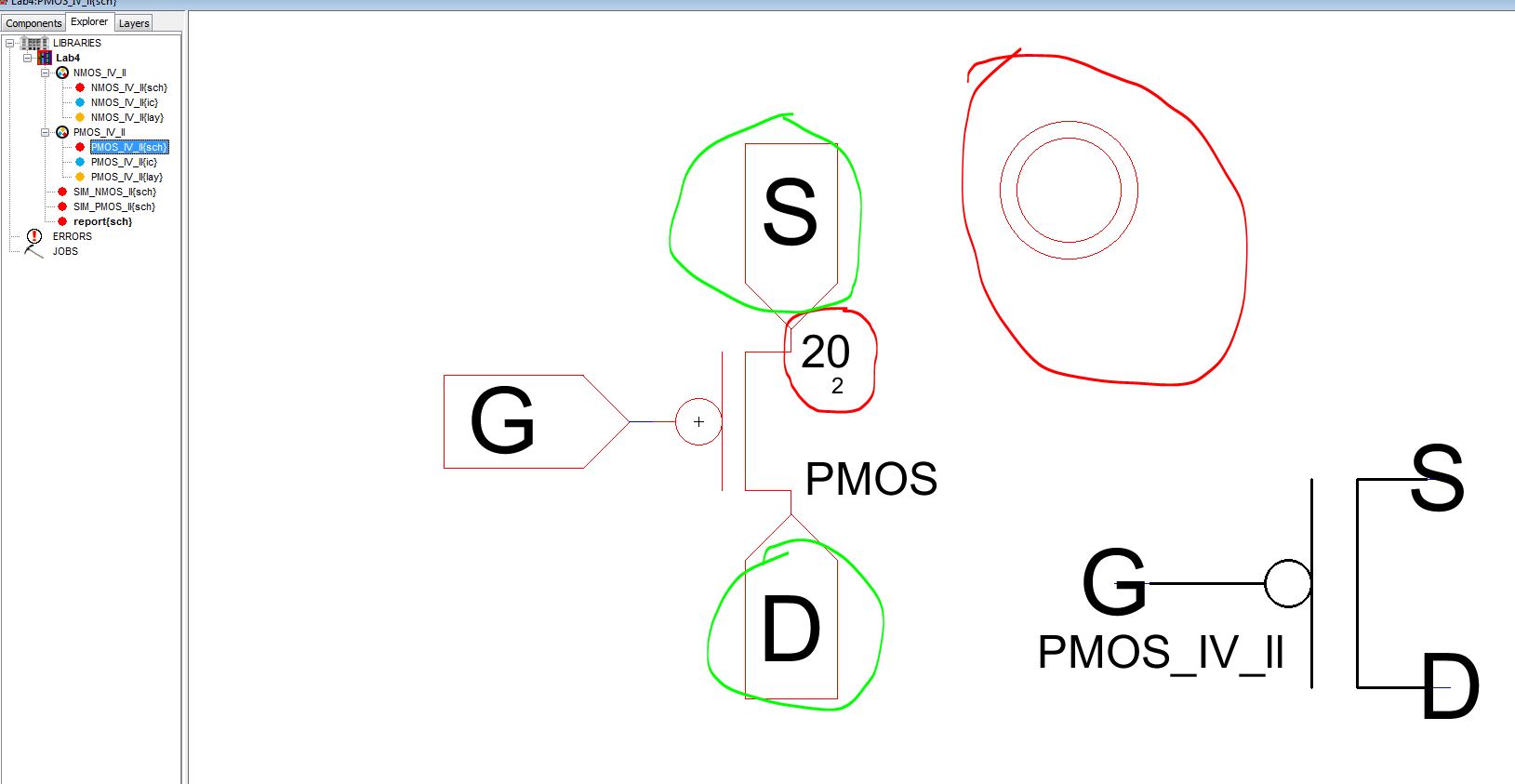
Notice that when making a PMOS schematic we add a power symbol instead of a gnd symbol (Circled in RED). Notice the size of the PMOS is 20/2 (circled in RED). Also note the orieantation of the source (S) and drain (D) pins (circled in Green).
Do a DRC check.

Making the NMOS Layout:
First we need 5 parts ,1 nMOS ,1 pwell ,2 nAct,and 1 polysilicon.

Next connect the nAct to the NMOS. Then connect the polysilicon to the pink part on the NMOS and Drag the pWell over to touch the pWell of the nAct

Change the size of the transister, nAct, Pwell to have a x value of 10. Connect metal 1 to the nAct and polysilicon and create exports.


Last DRC, do an Nwell check and NCC to make sure exports match.

View 3D results

PMOS layout:
PMOS is made in the same way except some minor changes.
it is made from 1 pMos, nWell, 2 pAct, and polysilicon

Notice the width of the PMOS and the pAct is 20, and the nwell is 10. Last create exports and name the spice model PMOS

Check DRC, NCC and well check.

View 3D results

Next we will take the Icons that we made and make a simulation profile for the transistors
NMOS

results

PMOS
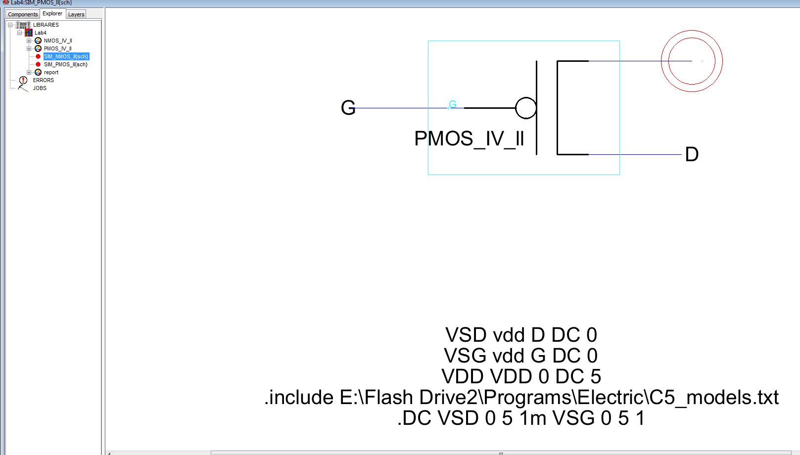
results

Last save and back up my files!!
