Lab 7 - ECE 421L
Authored
by Aran Johnson
Email: john1701@unlv.nevada.edu
October 18, 2013
Lab
description:
In this lab experiment we will:
-make a more concise schematic and icon for a 4 bit inverter
Prelab work:
-the prelab for this lab was to first work through Tutorial 5 which can be found here.
-as usual we were next instructed to back up all work previously done.
-finally we were instructed to read through the lab before approaching any of it.
Lab steps:
We start the lab by constructing a four bit inverter, as you can see below this can start to
get very bulky without the use of buses.
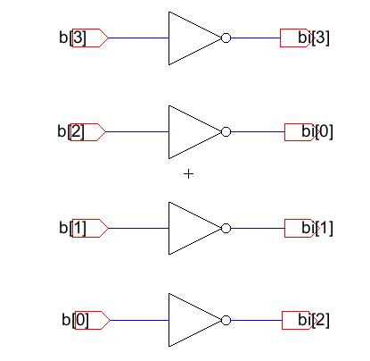
We can make this schematic much easier by creating a bus and using only one inverter icon.
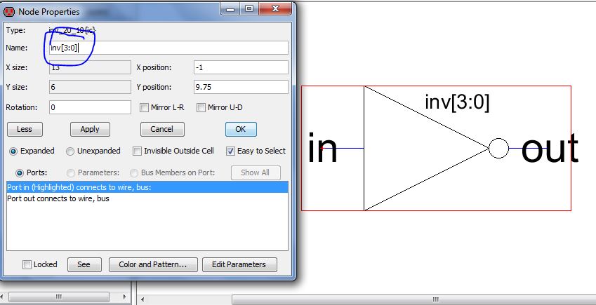
Our next step will be to create a new cell, making sure to put our initials and semester in
the name of the schematic, we will name the inverter inv[3:0].
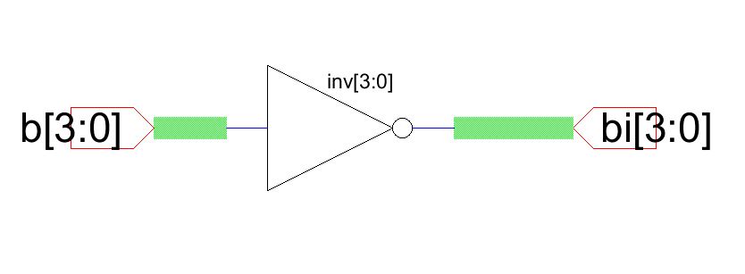
We now create two exports, one for the input and one for the output, naming the input b[3:0]
and the output bi[3:0], and then use the bus connection to connect the inverter to these exports.
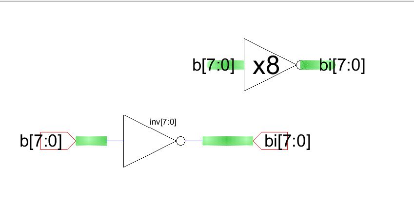
We now need to adjust this inverter to an 8 bit inverter, because 8 bit inverters are very important
in things such as ALU's, for operations like subtraction, we then create an icon for easier use later.
We can now simulate this circuit to test whether our bus connections are properly working, starting with a
new sim file. We use the icon for this circuit to build the new sim schematic.
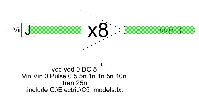
Our results confirm our expectations, each of our outputs are complements of the input.
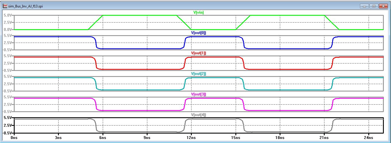
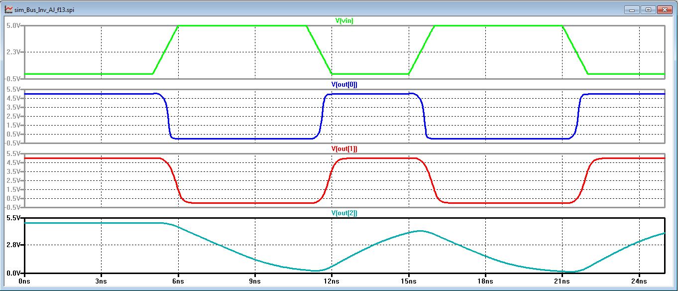
We now take different bits from the bus and tie them to different valued capacitors to see how the inverter will drive
them.
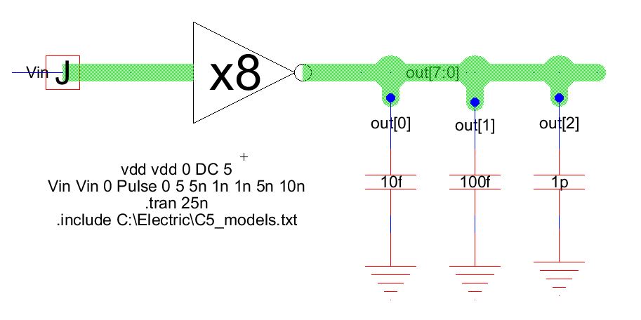
We see in the simulation results that the higher the capacitance value, the longer the output takes to reach its final
value.
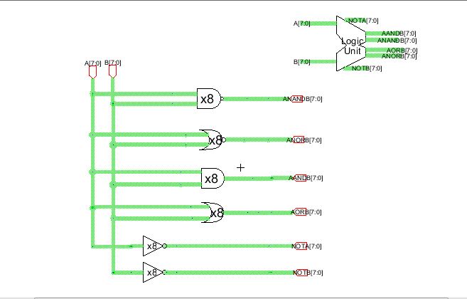
Our next step is to perform this same procedure for NAND, NOR, AND and OR gates to see what sort of outputs we
get and place them all in the same schematic to see if our simulations work together, as they will be required to in an
ALU.
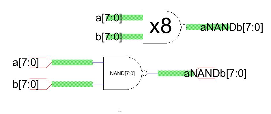
We start with the NAND gate, we place an 8 bit bus to both the a and b inputs.
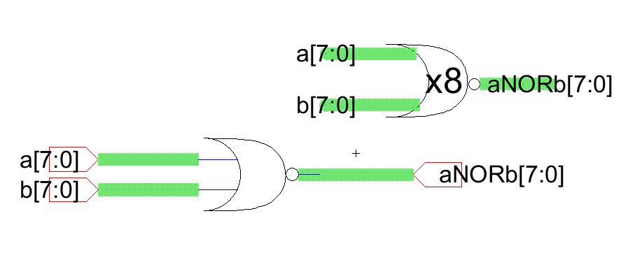
We will place this in a simulation file and move on to the NOR gate.
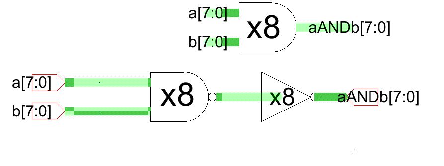
Now the AND gate, this will require the use of an inverter and NAND gate.
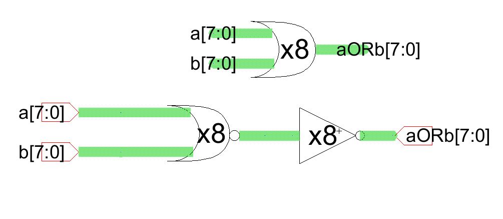
Finally we can now create our OR gate with buses using a NOR gate and Inverter.
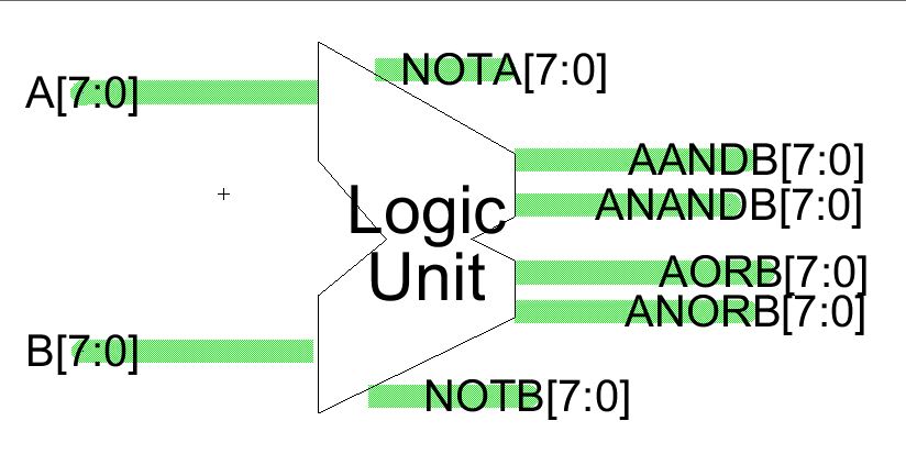
Now
we will move on to simulating each of these gates, to make things
easier we will put them all into one schematic and simulate them
simultaneously. We will start with the schematic.

After making the schematic and performing DRC on it we can move onto the Icon for it.
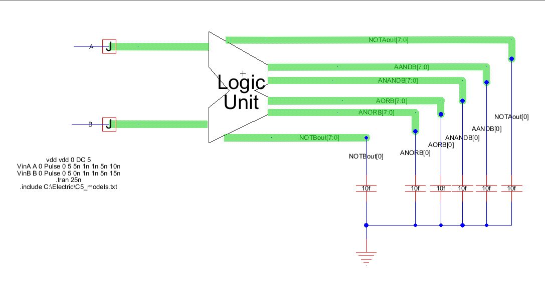
We then simulate the circuit to check if the logic values are correct, with a 10f capacitor to get a fast response.
I did two seperate pages of simulations because all of the graphs would not fit nicely onto one page.
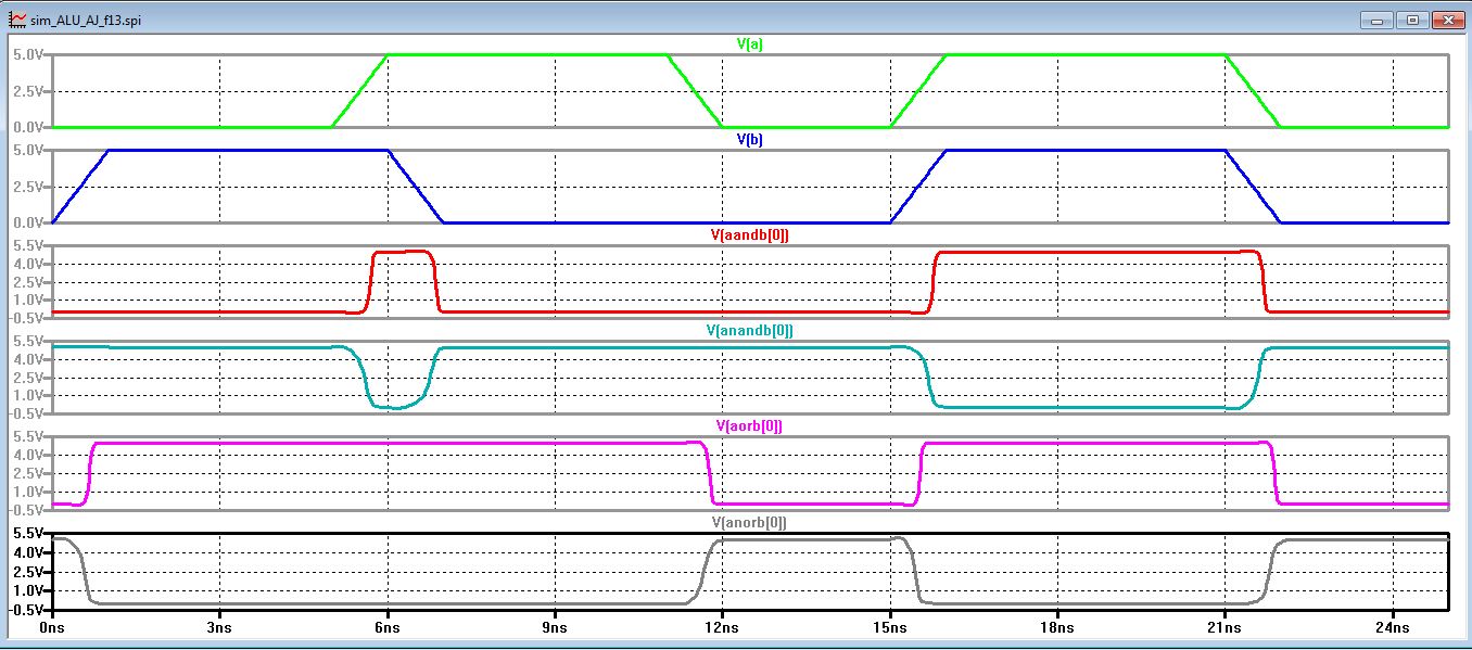
Here we can see that the AND, NAND, OR and NOR values are correct.
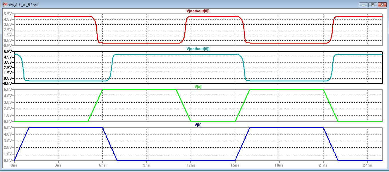
And here we see the correct NOT values are displayed.
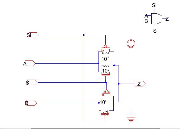
Next we will construct a Demux using MOSFETS, below is the schematic.
The next step is to create an icon to simplify the simulation.
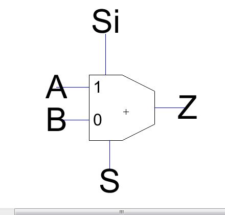
A Demuliplexer works with the input S acting as a selector pin that will select the input (A or B) that
is passed through to Z, we will simulate to see if it behaves in this manner.
As
you can see in this simulation, when a logic value of 1 is seen on the
S pin, A is passed through to Z, when a 0 is seen on S B is passed
through to Z.
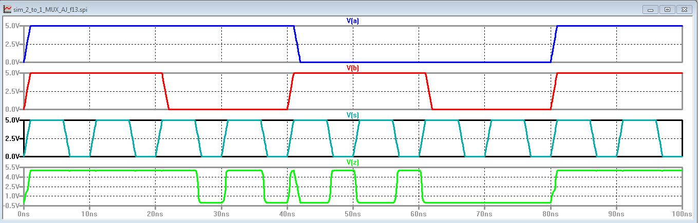
We will now simulate the operation of the Demux when it is in the Mux orientation.
We
can see here that when a logic value of 1 is on the S pin then the A
output is selected to pass the Z input and when the 0 is selected
the Z input is passed to the B output.
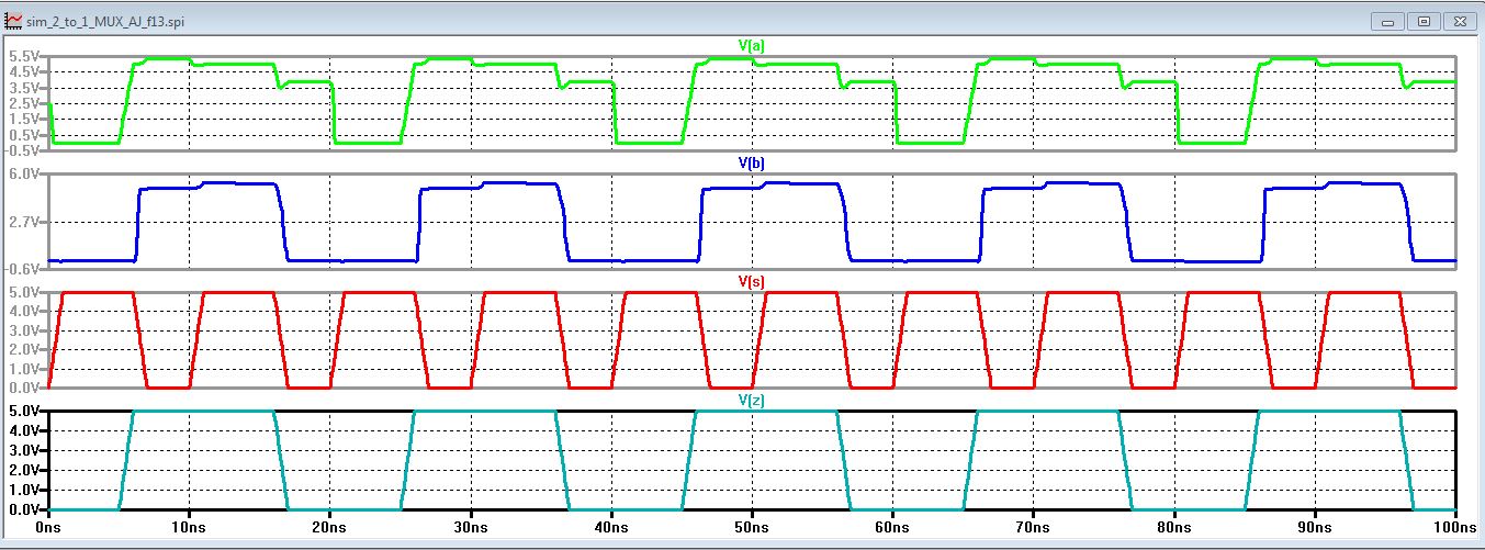
Now we will construct an 8 bit wide Demux/Mux, we will use a bus to implement the design.
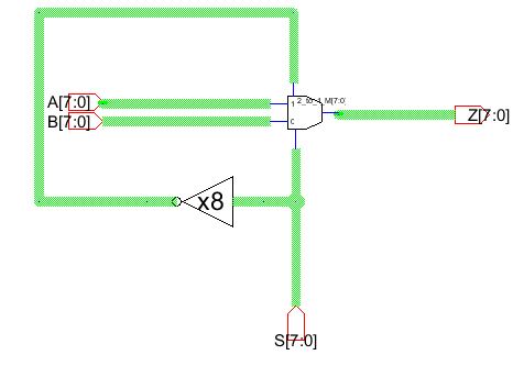
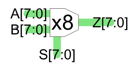
Next we will again build an icon to more easily simulate this circuit.
Now we will finally simulate it to make sure it works correctly.
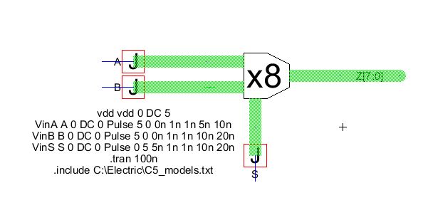
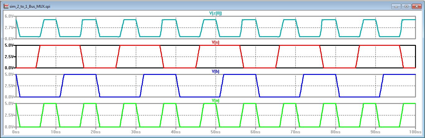
Using this simulation we can see that the output matches the same behavior as the previous 1 bit Demux.
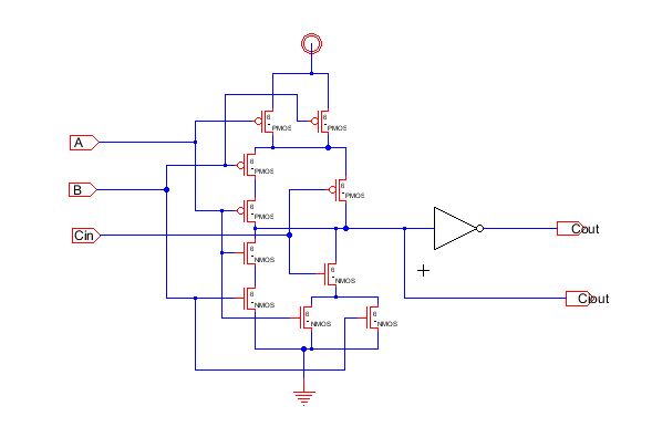
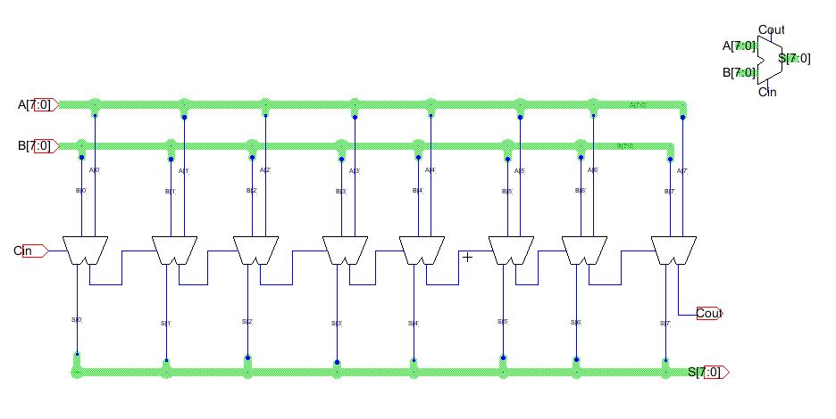
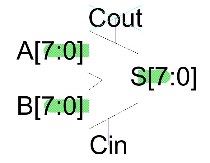
Our
final task will be to construct an 8 bit full adder, this will require
a little more work because the Cin's and Cout's of the 2nd-7th
adder
must
connect together. We will begin by constructing schematics and
simulating the Summer and Carry circuits and then implement them
into
one final design that will be repeated 8 times.
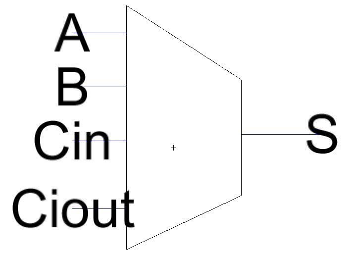
First we have the Carry circuit.
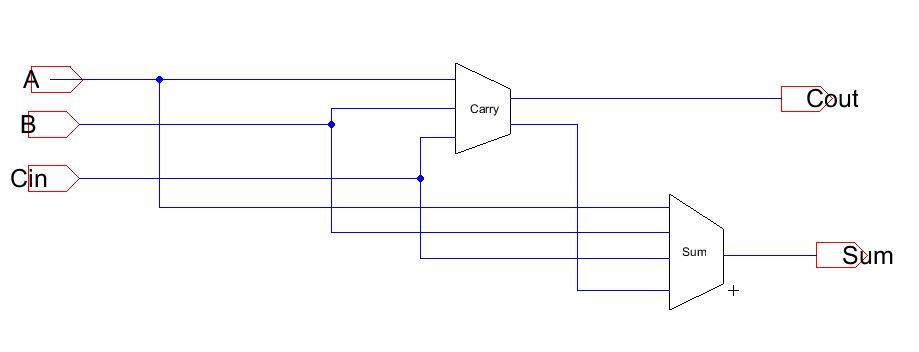
Now we will build the Summer.
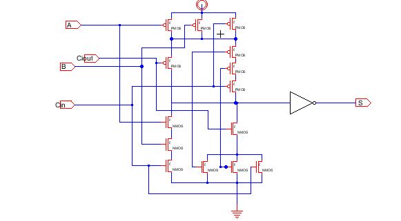
We will build icons for each of these circuits making the final circuit simpler.
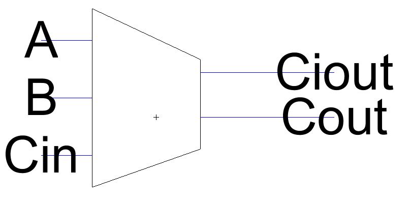
We implement these into one full adder circuit.
Using this, one more icon can be put together to be put into the 8 bit schematic.
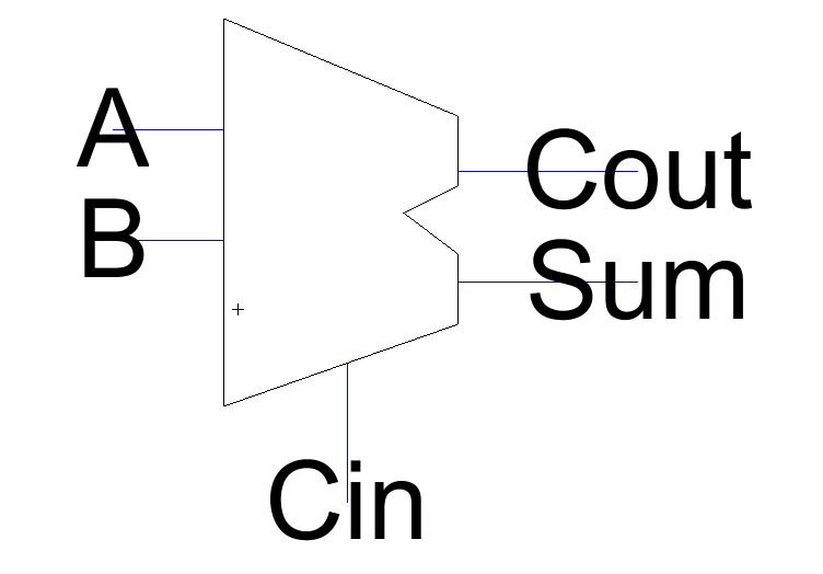
Finally we will put this into one schematic to implement the whole 8 bit Full Adder.
One more icon can be created for simulation to verify the schematic.
Below is the simulation results to verify this circuit.
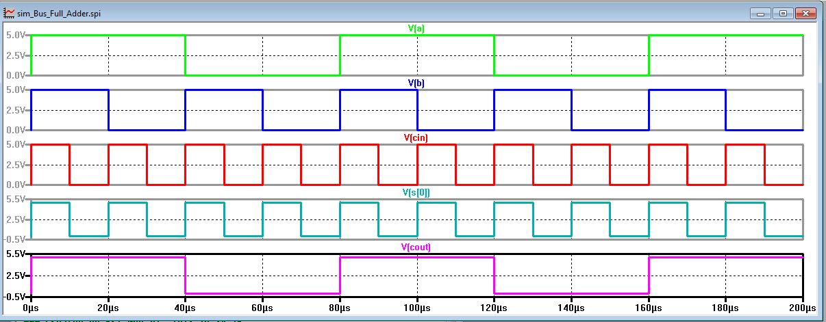
Our
input to this circuit was a junction with a pulse alternating for A and
a faster pulse for B to get different values. The design was
verified by taking one point such as at 60 us to 80 us the value of A
is 0 and the value of B is 0 with a Cin of 1 which should mean an
output of 1. This
verification was done multiple times giving us the conclusion that it works.
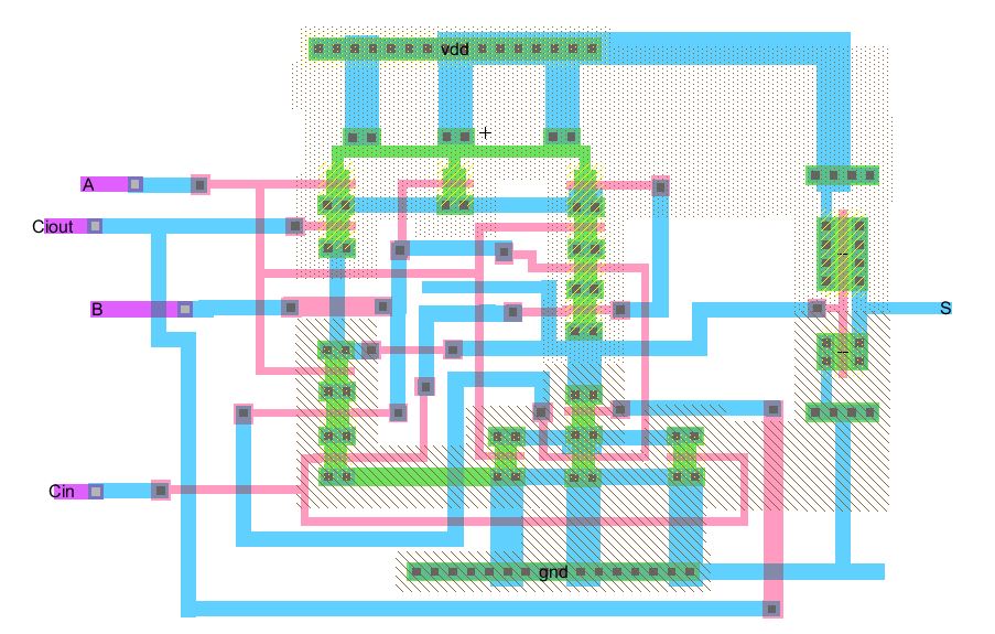
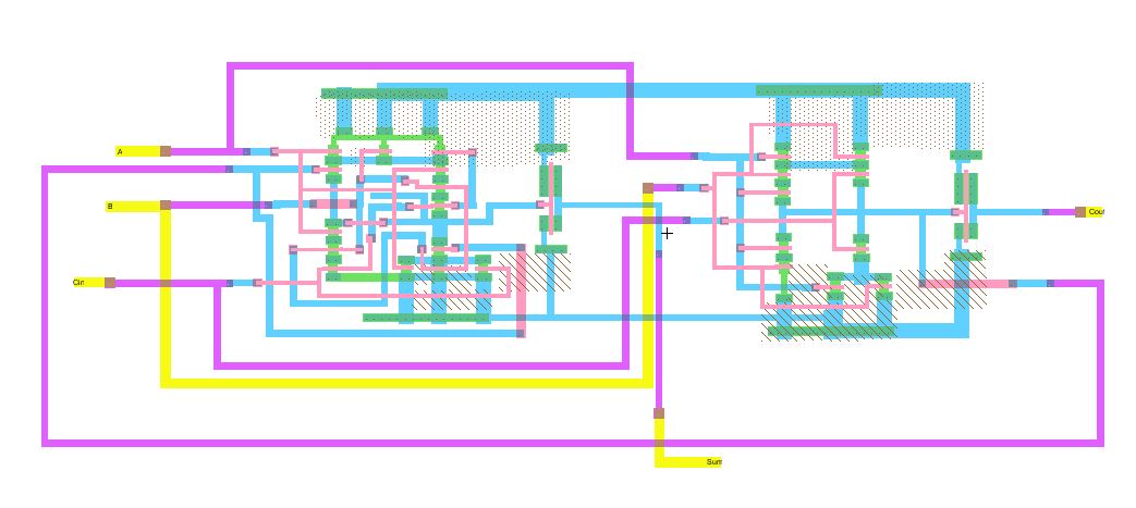
Our final task is to layout the 8 bit full adder we will start with the layout of the summing portion of the adder, and
move on to the carry and then create duplicates for each bit.
Below is the summing layout, after it has been NCCed ERCed and DRCed.
Next is the layout of the carry bit.
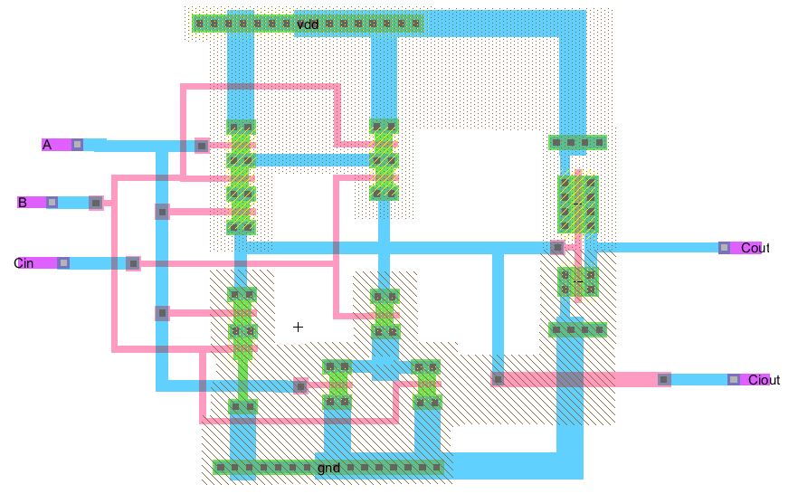
Next we place these into one schematic for a full adder, like how we did with the schematics earlier.
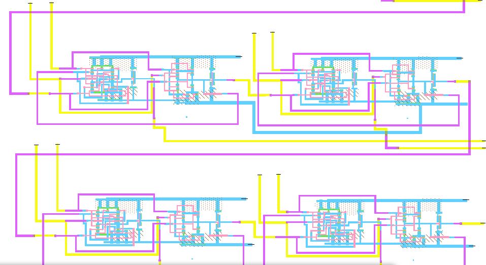
Finally
we can place eight of these full adders together, interconnecting the
carry bits correctly and we have finished with the
layout of an 8 bit full adder.
.jelib
Return