Lab 5 - ECE 421L
Authored
by Aran Johnson,
Email: john1701@unlv.nevada.edu
October 4, 2013
Lab
description:
In this lab experiment we will:
-put together a schematic for a 20/10 sized inverter using PMOS and NMOS transistors
-put together a schematic for a 100/50 sized inverter using PMOS and NMOS transistors
-create icons for both inverter setups
-simulate these inverters driving capacitors of different sizes in spice, ALS, and IRSIM
-build the layout of both inverter setups.
Prelab work:
-the
prelab was to go through Tutorial 3 to gain an understanding of how to
layout and build a schematic of inverters in the C5 process it is seen here.
-also backup all previous work
Lab steps:
We will start by placing two transistors, one PMOS and one NMOS, we will connect the gates of both
together and the drain of the NMOS to the drain of the PMOS and take our output from this node. Then
the source of the PMOS is connected to Vdd and the source of the NMOS is connected to ground which should look like this.
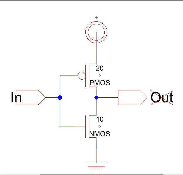
We change the widths of the PMOS and NMOS to 20 and 10 respectively, with lengths of 2. We can now
set spice models for each transistor using the C5_Models.txt file as we did in the previous lab, and export
our In and Out pins.
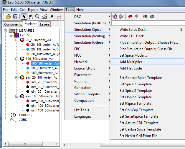
Now we will put together our 100/50 Inverter using a multiplier on both PMOS and NMOS transistors.
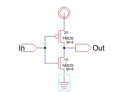
To set the multiplier to 5 we must navigate to Tools->Simulation(Spice)->Add Multiplier
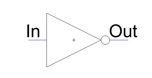
In order to make our future simulations simpler we will now create icons for these two schematics.
They will be in the shape of the logic symbol of an inverter to make things easier.
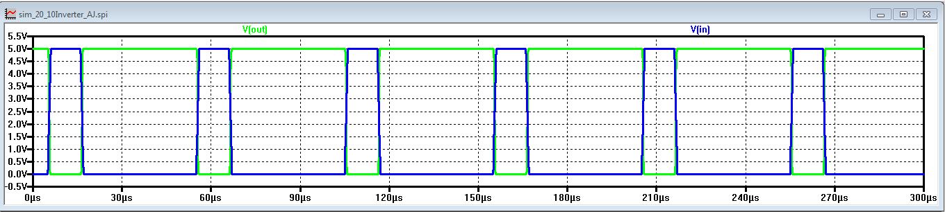
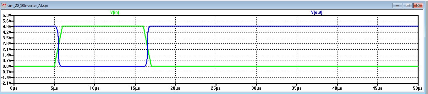
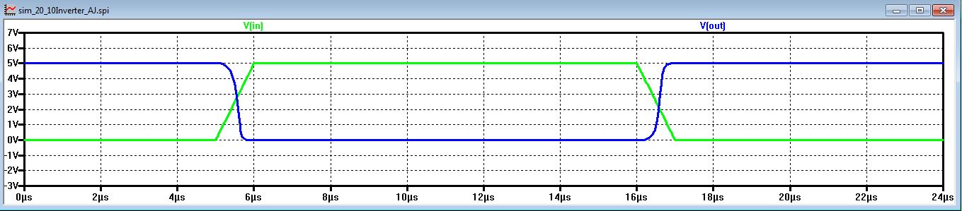
We can now simulate the schematic for this circuit driving different sized capacitors. Starting with a
100fF capacitor, and then a 1pF and 10pF. First for a 20/10 and then the 100/50.
From
the results we can see that the smaller the capacitance value the
faster the rising time of the inverter will be. This is most
likely due the lower charge requirements of smalller capacitors.
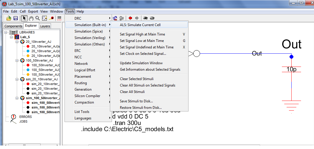
We
can now ALS simulate the schematics by first setting exports on the
schematic and selecting Tools->Simulation(Built-In)->ALS:Simulate
Current Cell. We can now set the input high by selecting it and
moving the dotted line and pressing 'V' for high and 'G' for low.
This will allow us to see the output delay.
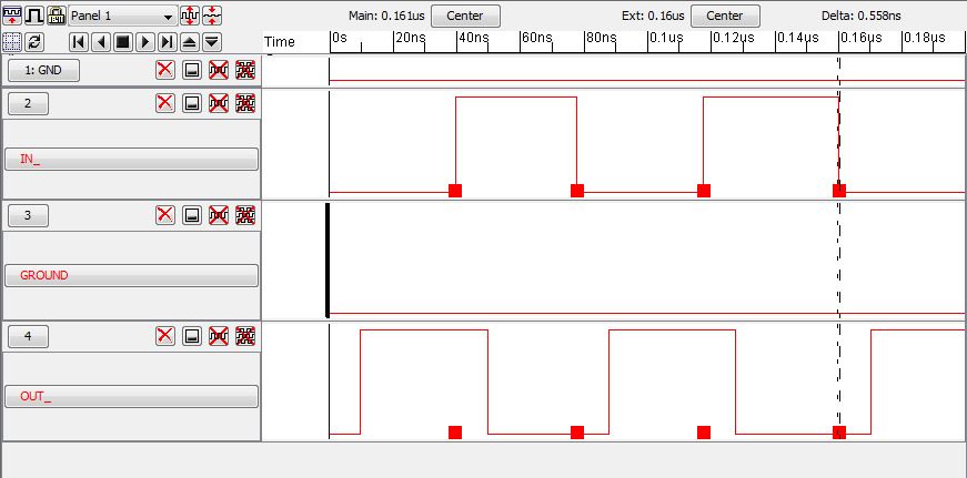
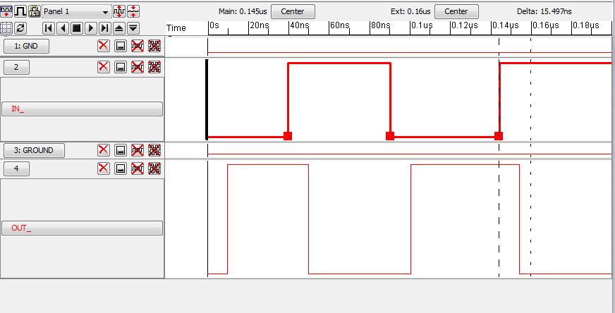
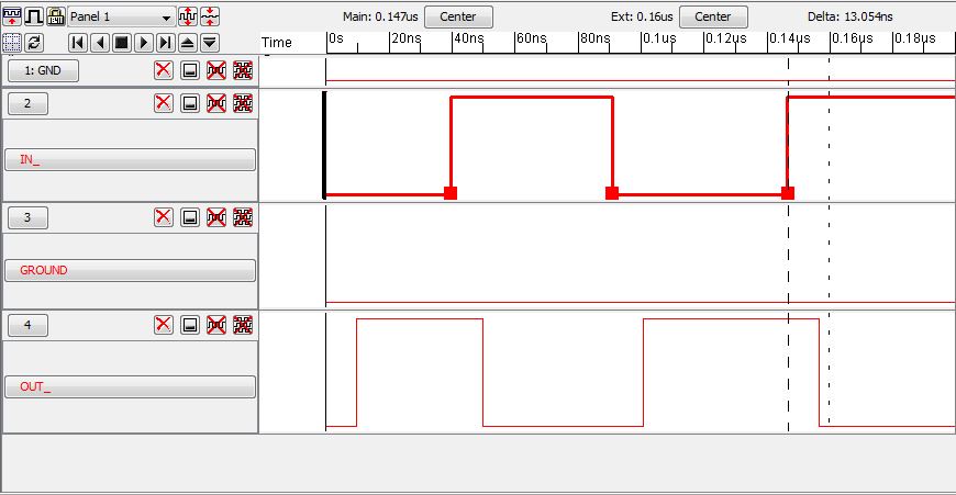
The delays don't look extremely different but as the capacitance increases there is a small increase in the time.
We can now layout our two inverters by placing NMOS and PMOS transistors and connected their sources and drains to
an
n-active and p-active to metal 1 nodes. We take the input to be
the poly layer that is placed as both transistors' gates,
and we take the output to be the metal 1 node exiting the NMOS and PMOS transistors' drains.
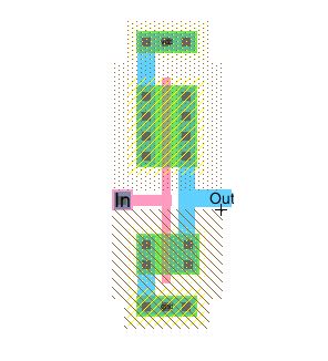
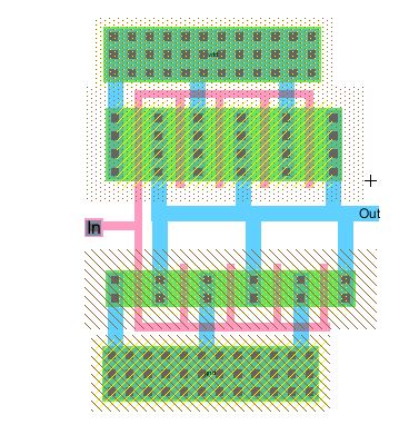
We must make sure to not forget the p-well and n-well nodes that will act as our vdd and gnd nodes.
Also we must also make sure we export the input and the output so that our layout will LVS correctly, from here
we will DRC to make sure our layout follows all of our design rules and ERC the layout for a well check, when this
is all done we are finished with our layout.
.jelib
Return