Lab 6 - ECE 421L
Authored
by Fred Hathaway,
hathawa6@unlv.nevada.edu
11 Oct 2013
Lab 6: Design, layout, and simulation of CMOS NAND/NOR/XOR gates and a full-adder:
In
this lab, I will be designing a CMOS NAND/NOR?XOR gate and a full-adder using Electric and
simulating them using IRSIM and ALS (asynchronchronous logic
simulator).
I completed the prelab and followed tutorial 4 and electric video_11.
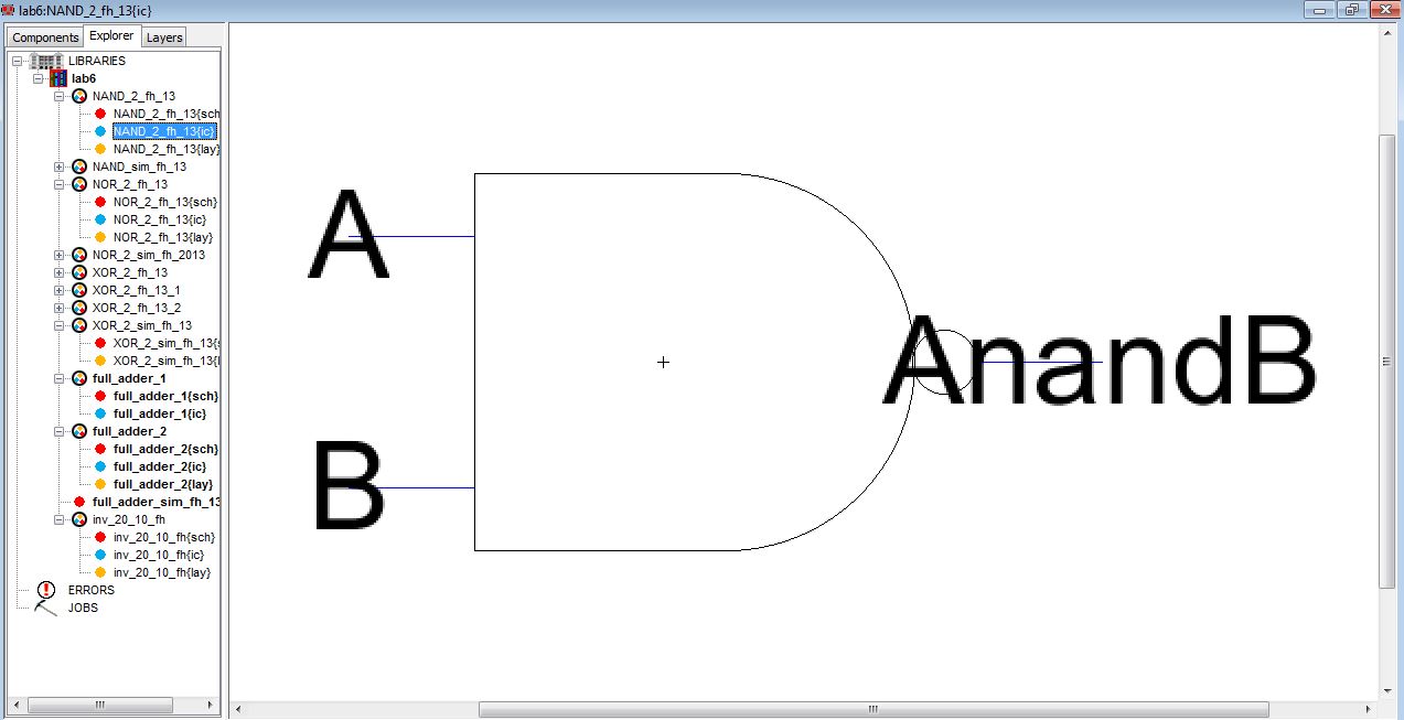
By following the prelab tutorial I was able to use the NAND gate that was I created from the tutorial. Both the PMOS and NMOS MOSFETS are 10/2. I also created an icon view seen below with the schematic view.
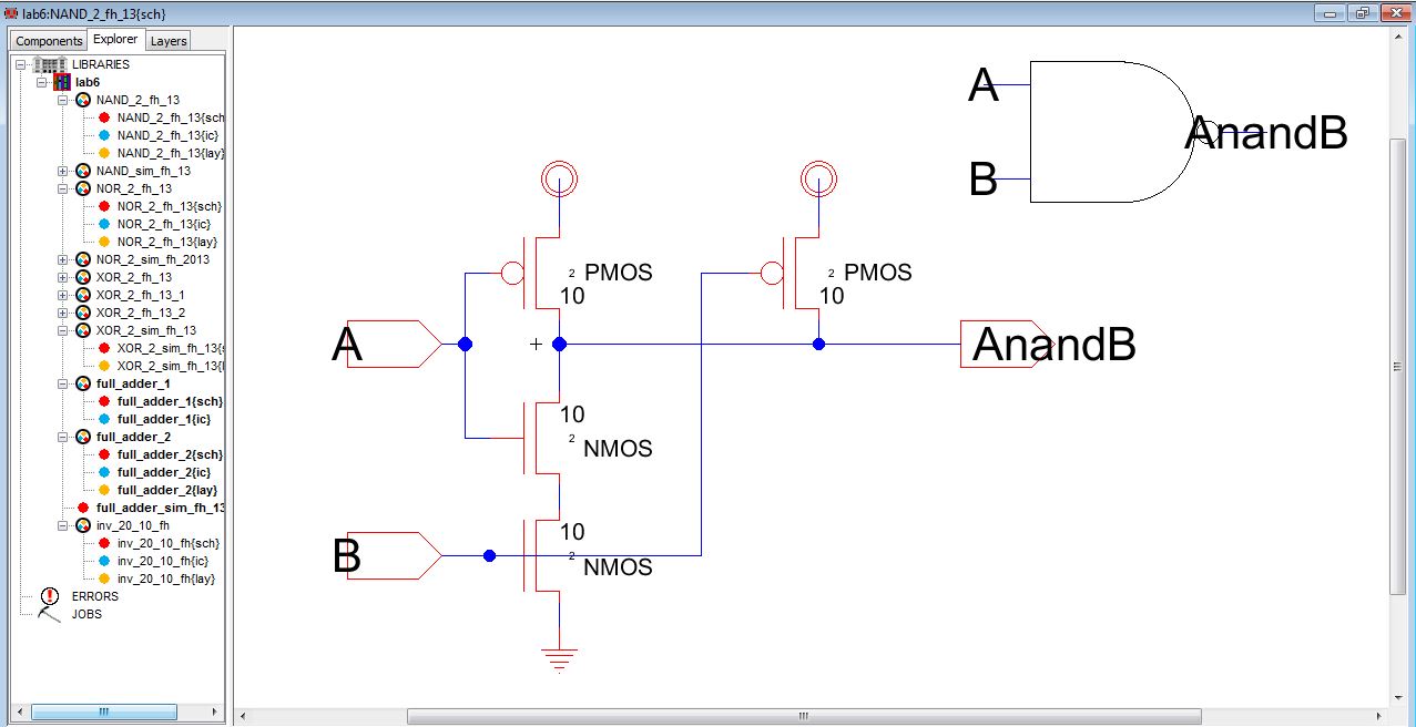
Notice
that the icon view is the commonly seen NAND gate. This will make
the schematic view look much better when we simulate.
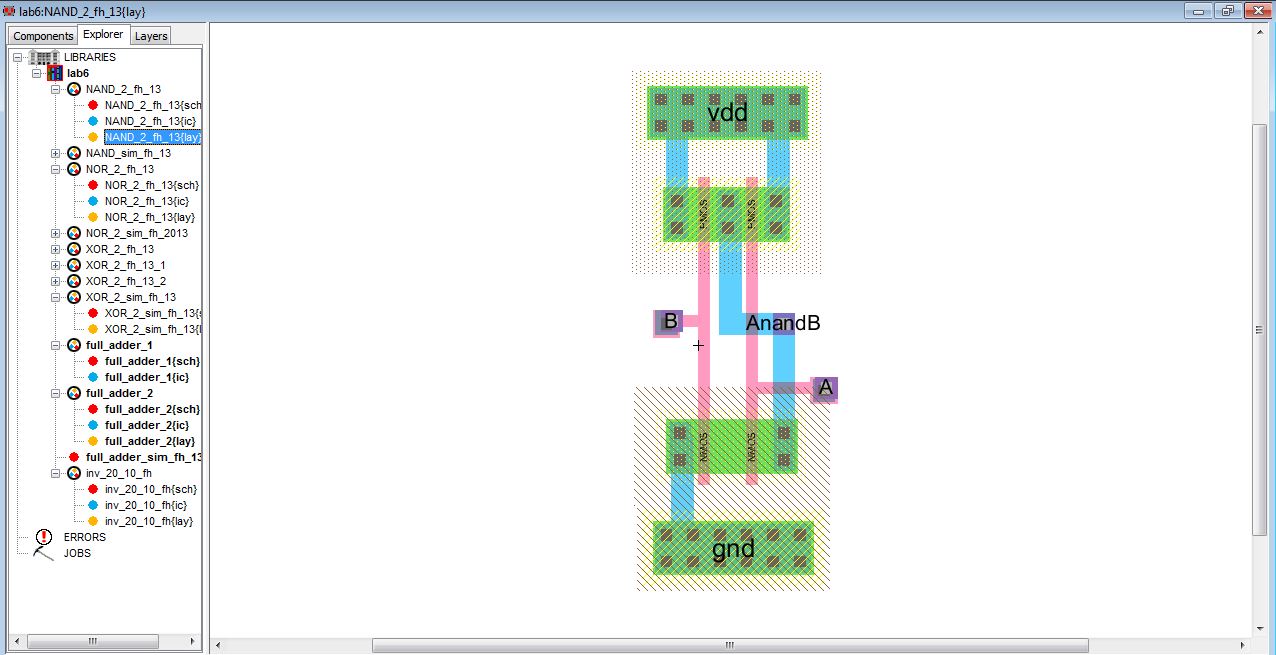
Next
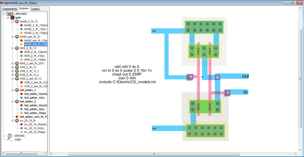
I created a layout for the NAND gate seen below. Check for DRC
and NCC errors. Correct any errors that you may encounter.
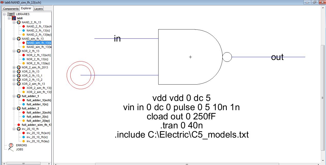
Next I created a simulation schematic with the icon that I created. Notice that I connected VDD to one of the inputs.:
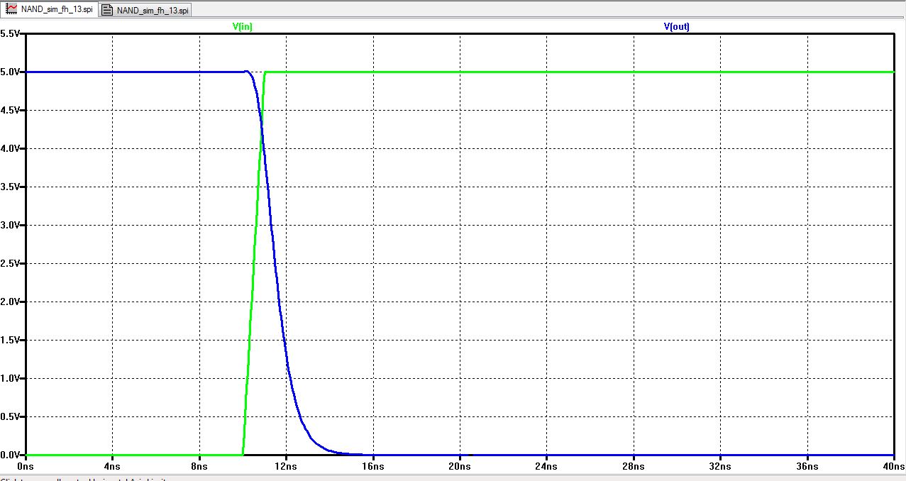
Seen below is the resulting waveform in LTSpice.
In
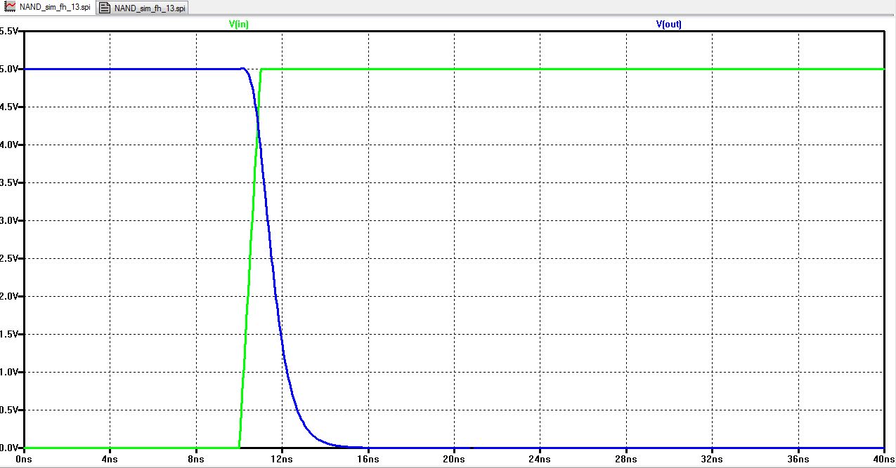
addition to the shematic simulation, I also created a layout sim cell
and ensured we get the same result for the layout cell. Notice
that the inputs and outputs are connected to metal1. Make sure to
check for ERC, NCC and DRC
The simulation results are what I expected.
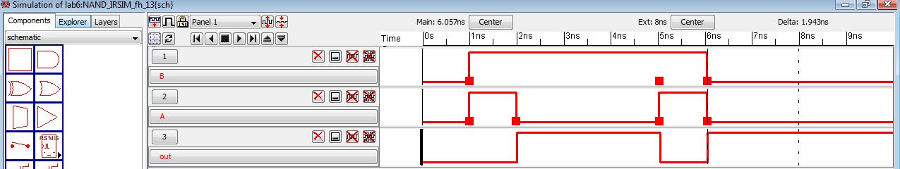
Next I created another schematic for IRSIM and LTSpice.
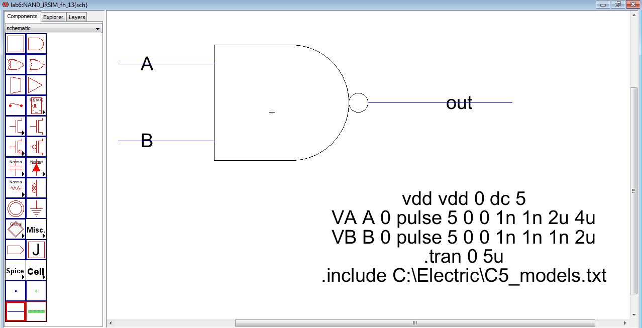
LTSpice results. We see what when both inputs are high, the output is low.:
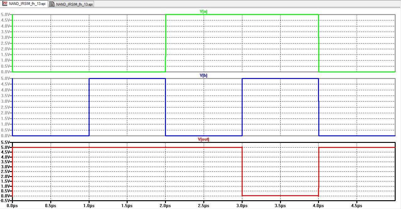
IRSIM results. As we can see when both inputs are high, the output is low.:
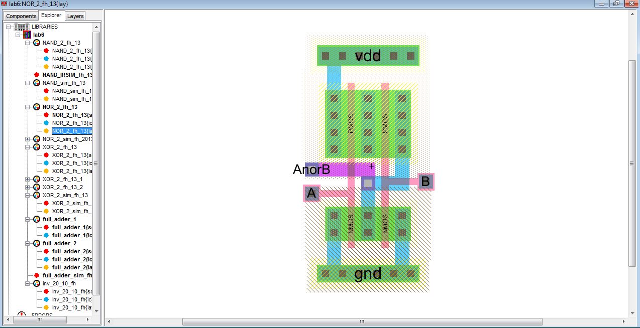
NOR gate:
For the XOR gate, I repeated the above steps to draft the schematics, icon and layouts.
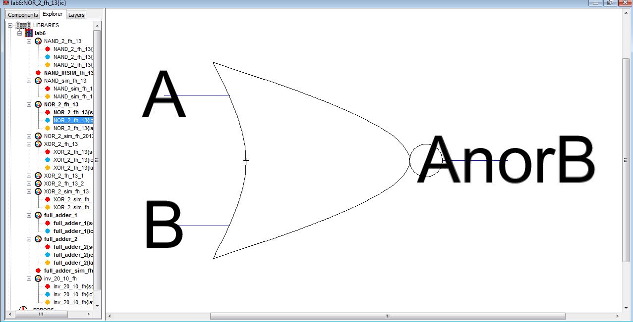
Icon for the NOR gate. Again I created an icon view that represents the common symbol for the NOR gate:
NOR layout:
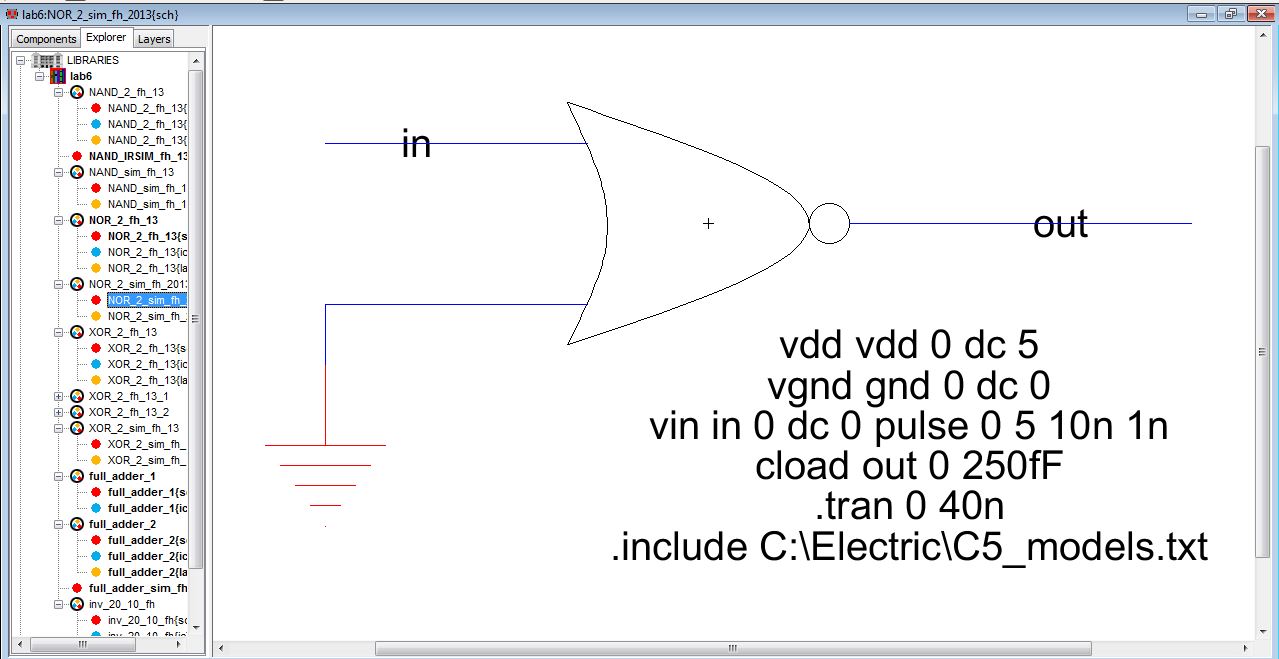
Schematic view for simulation:
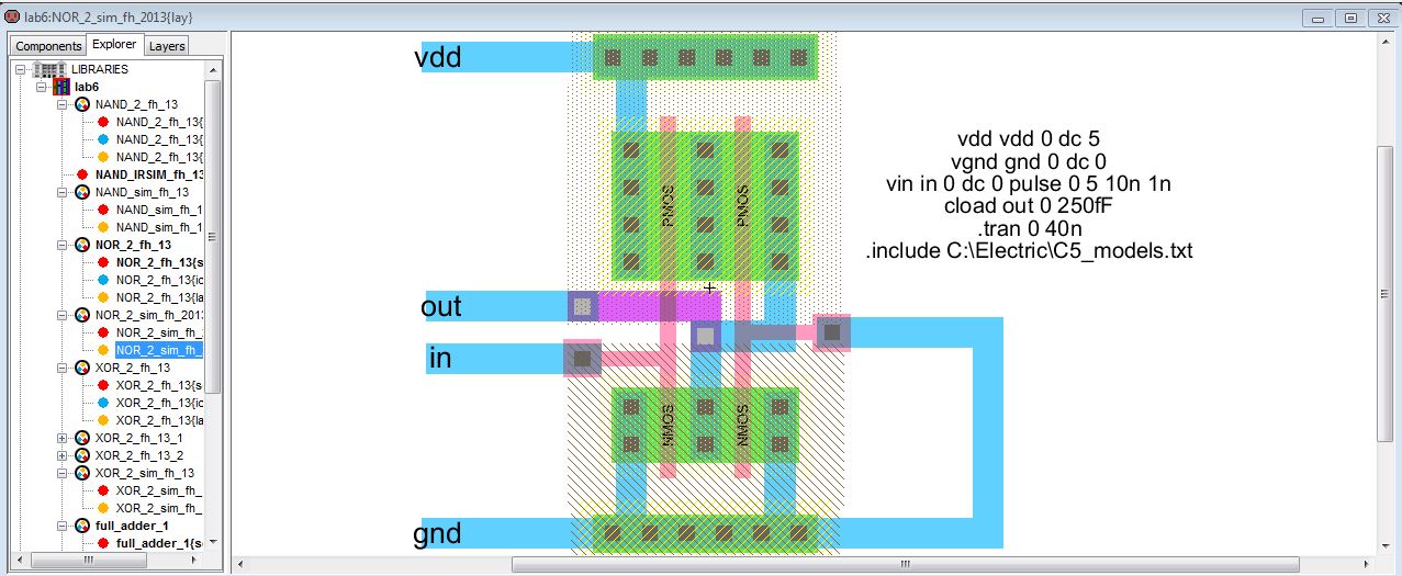
Layout view for simulation:
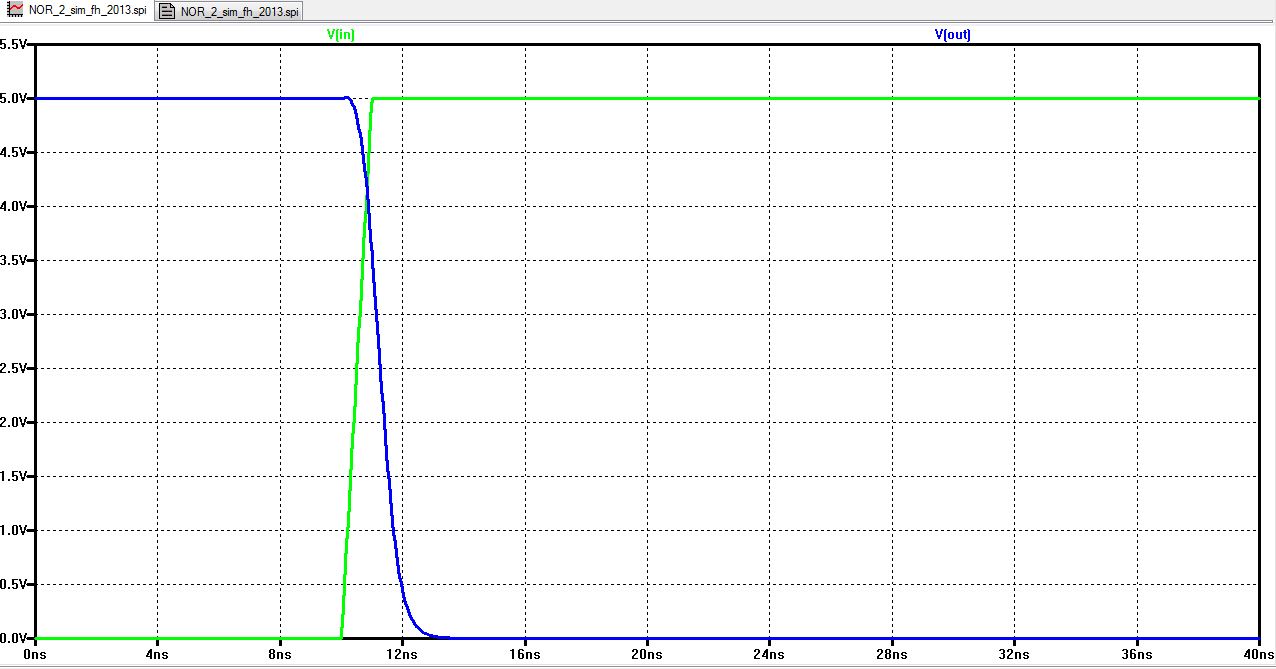
NOR simulation:
Next, I will create another schematic for the IRSIM and LTSpice for the logic simulation:
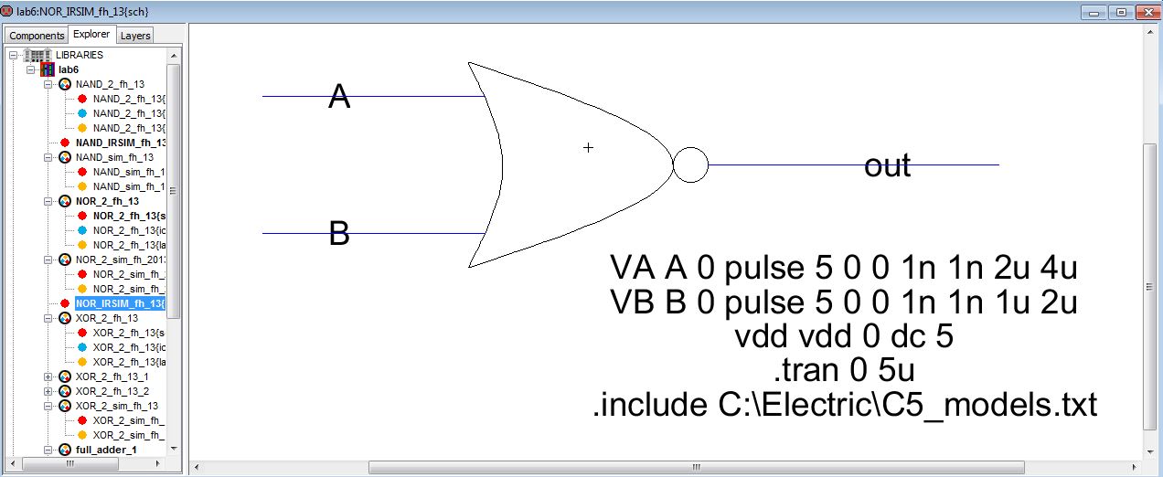
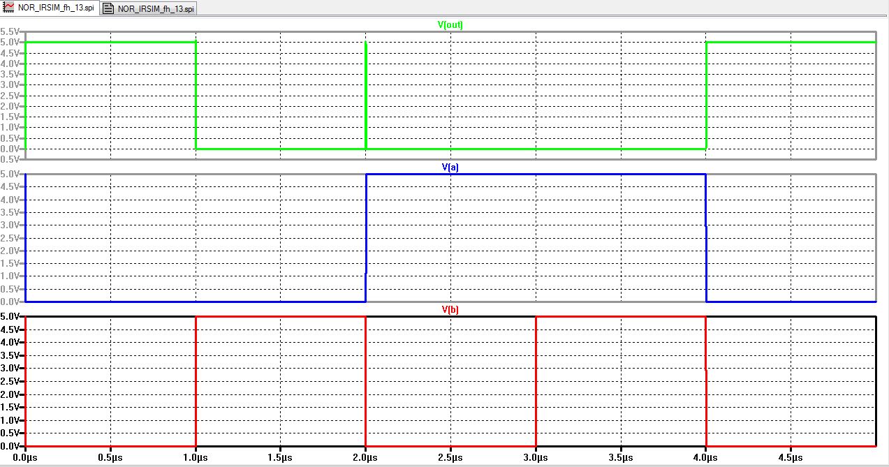
LTSpice logic simulation:
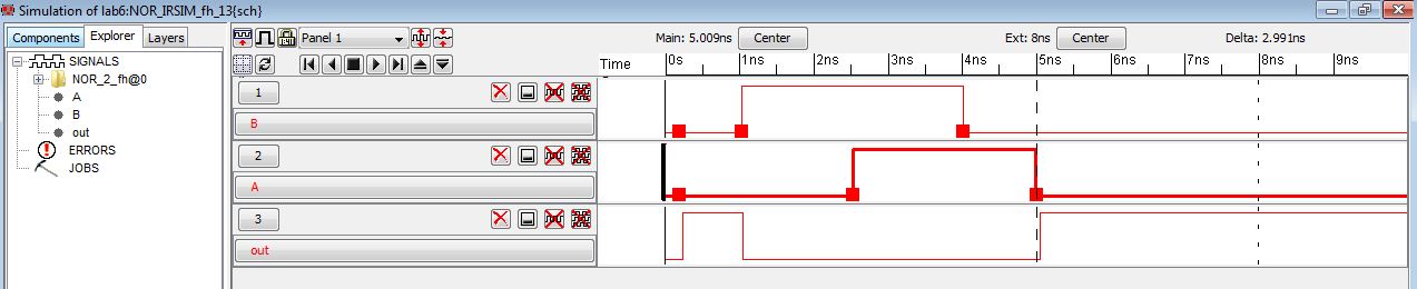
IRSIMfor NOR gate:
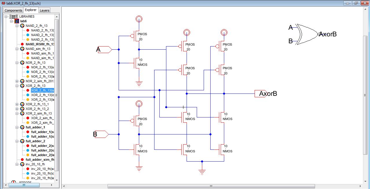
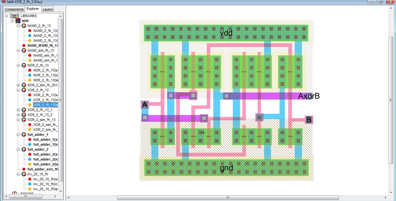
XOR gate:
For the XOR gate, I repeated the above steps to draft the schematics, icon and layouts.
Schematic view:
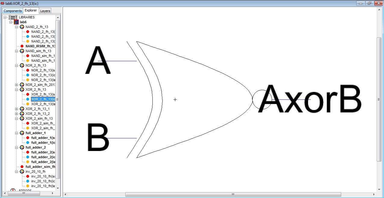
Icon view:
Layout:
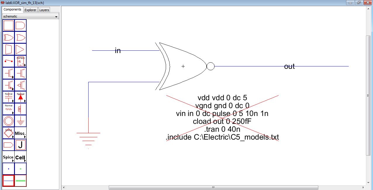
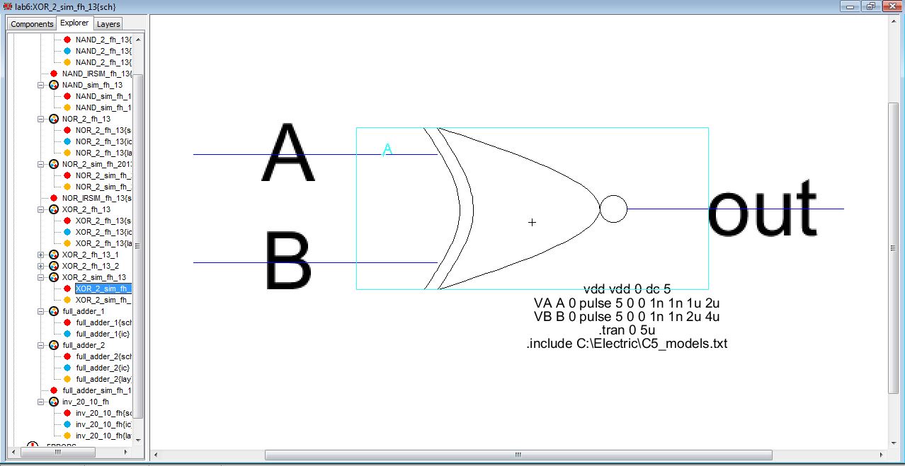
XOR simulation schematic:
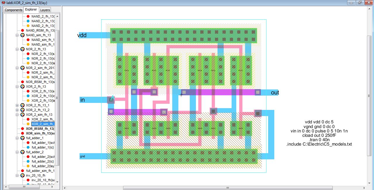
XOR simulation layout:
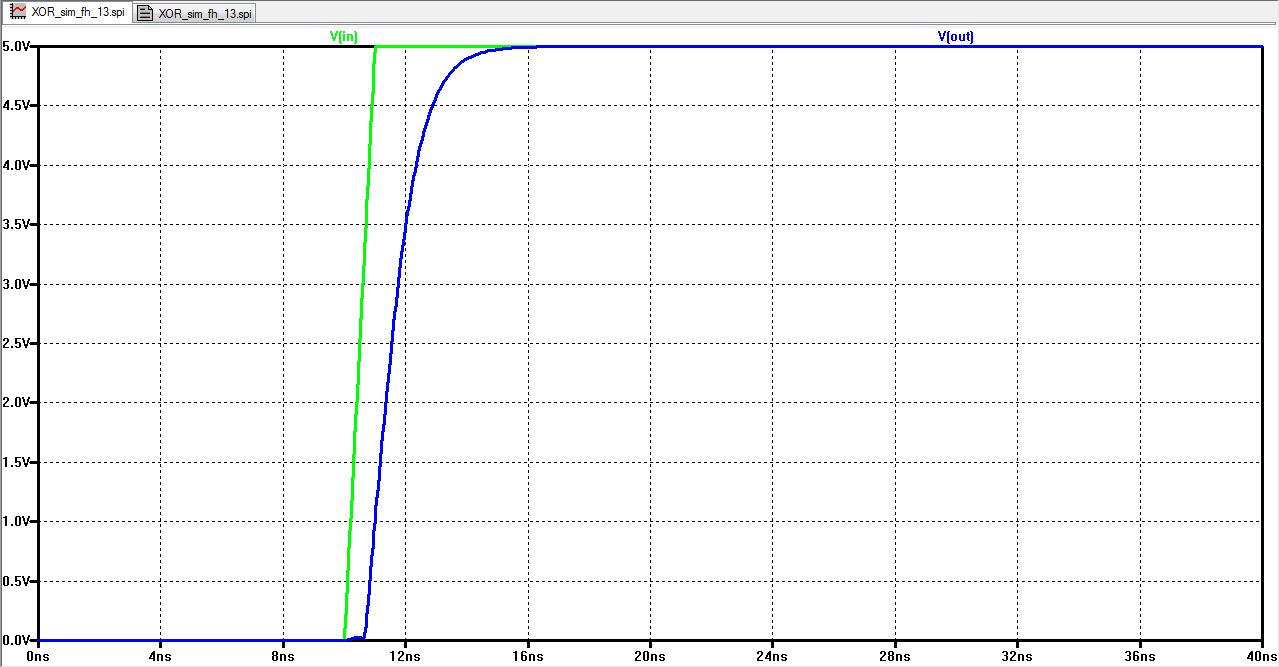
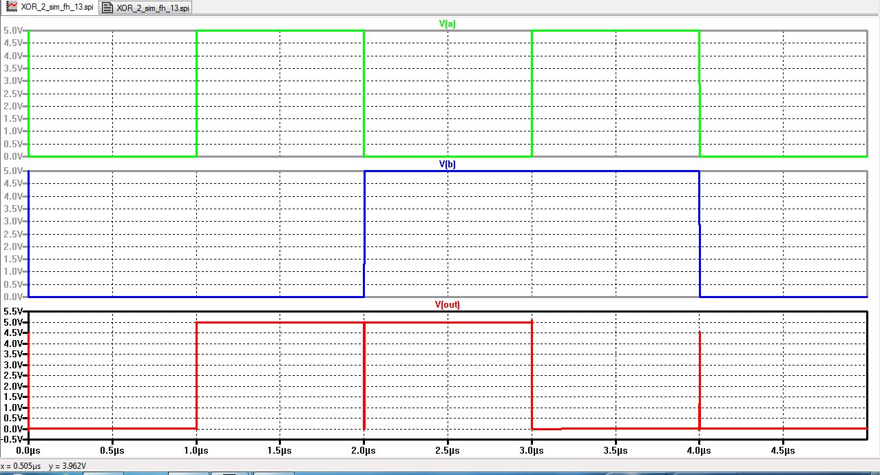
Simulation results:
LTSpice and IRSIM logic schematic:
LTSpice and IRSIM logic simulations:
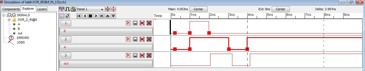
IRSIM results:
Full adder:
Next, I will create a full adder using the gates created above:
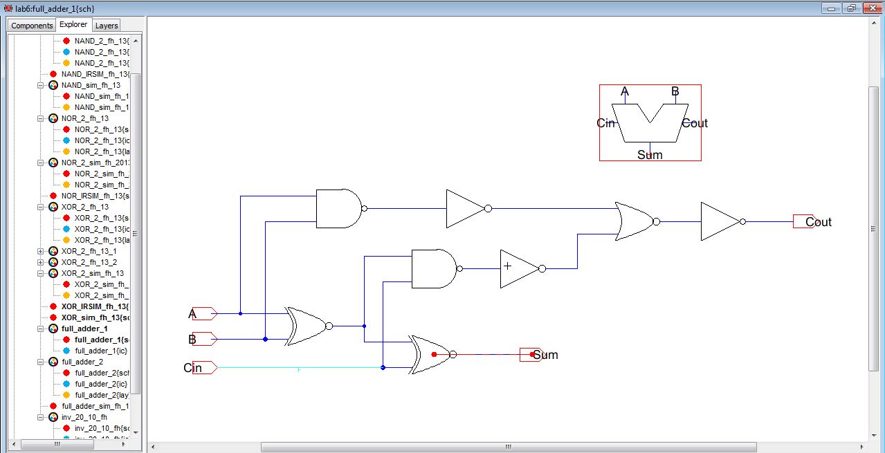
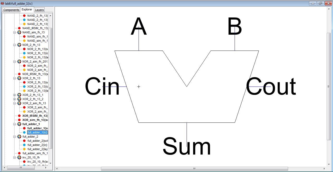
Icon for the full adder:
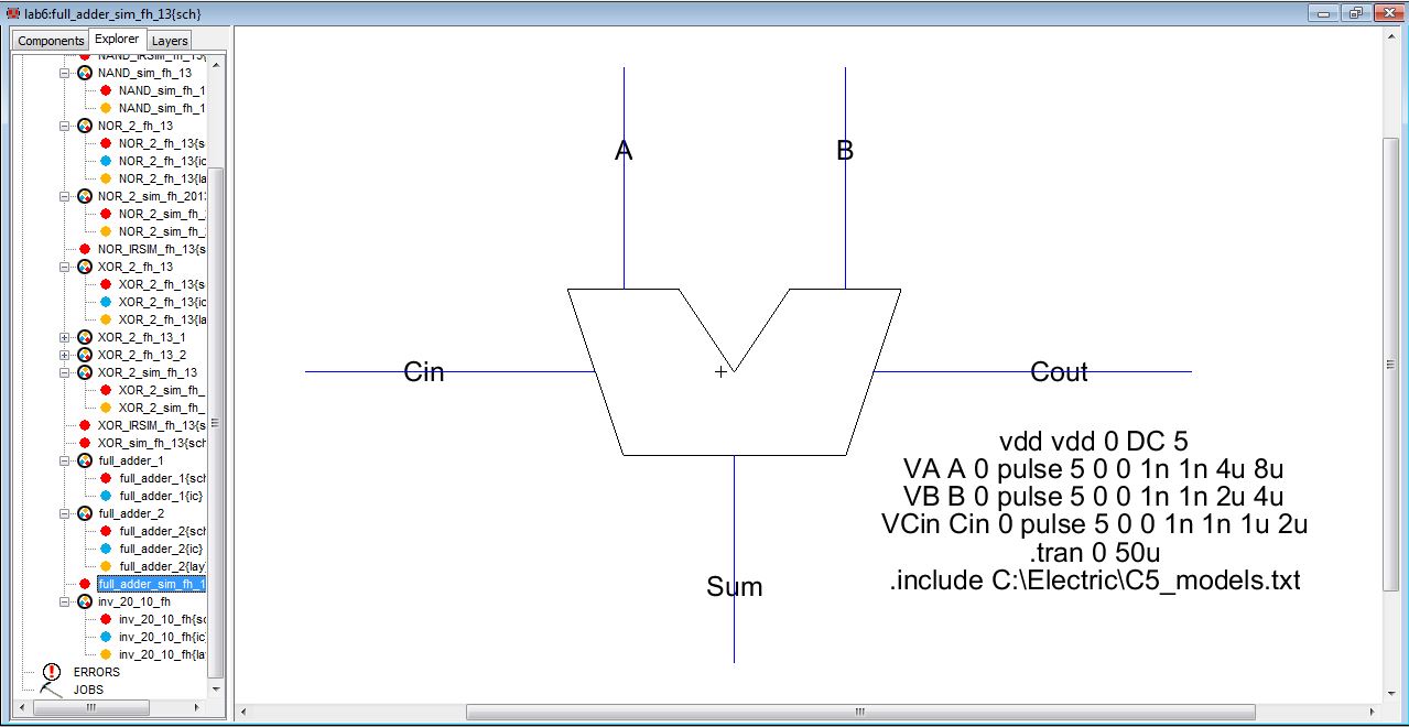
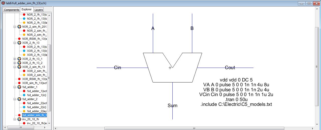
Full adder simulation schematic using the icon that I created:
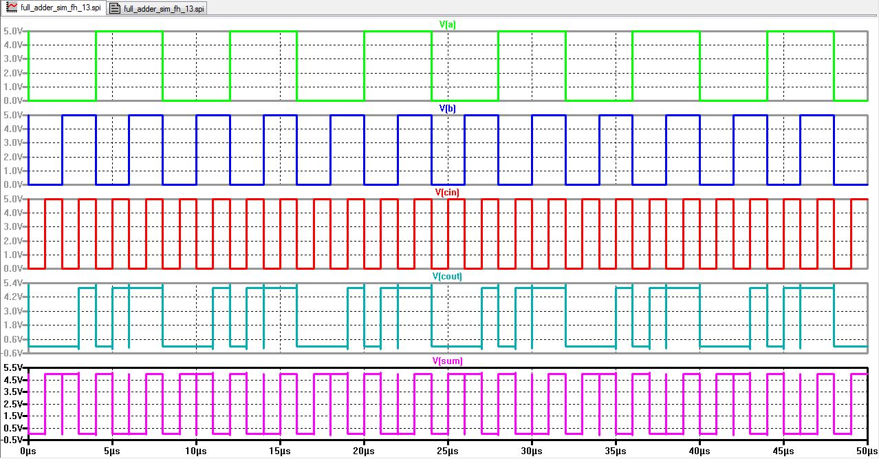
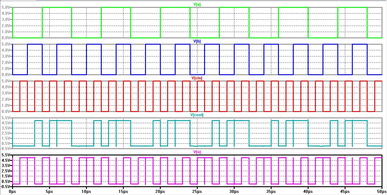
The simuation wave form:
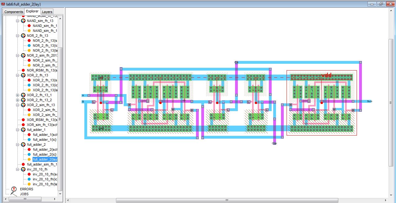
I designed another full adder using 3 NAND gates and 2 XOR gates:
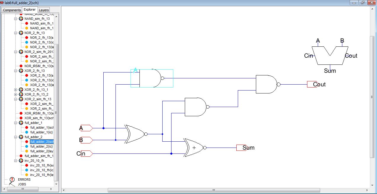
I used the same icon from the first full adder:
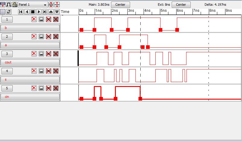
IRSIM schematic:
LTSPice logic simulation results:
IRSIM results:
I backed up my lab work by archiving directory, emailing and posting on the cmosedu website.
Copy of lab6_Hathaway.jelib file
Return to EE 421L Labs