Lab 5 - ECE 421L
Authored
by Fred Hathaway,
hathawa6@unlv.nevada.edu
4 Oct 2013
Lab 5: Design, layout, and simulation of a CMOS inverter:
In
this lab, I will be designing a CMOS inverters using Electric and
simulating them using IRSIM and ALS (asynchronchronous logic
simulator).
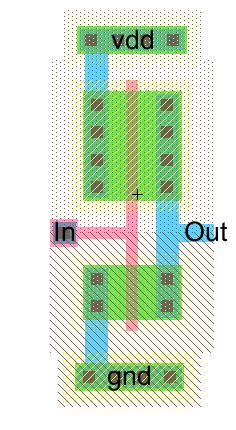
To draft the schematics and layouts I followed tutorial3 from CMOSedu website. The PMOS transistor has a width of 20 and a length of 2. The NMOS transistor has a width of 10 and a length of 2.
To
change the width of the PMOS and NMOS transistors, used CTRL-I and edit
the properties of the transistors. Additionally, we need to go to
Tools->Simulation (Spice)->Set Spice model. Then we need to
press CTRL-I to set the spice model to PMOS and NMOS. You can
also create an icon view. To make icon view click on
View->Make icon view. I am not going into detail on how to
draft the schematics since you can refer to the tutorial 3 video. Below
is a snap shot of my schematics.
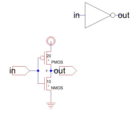
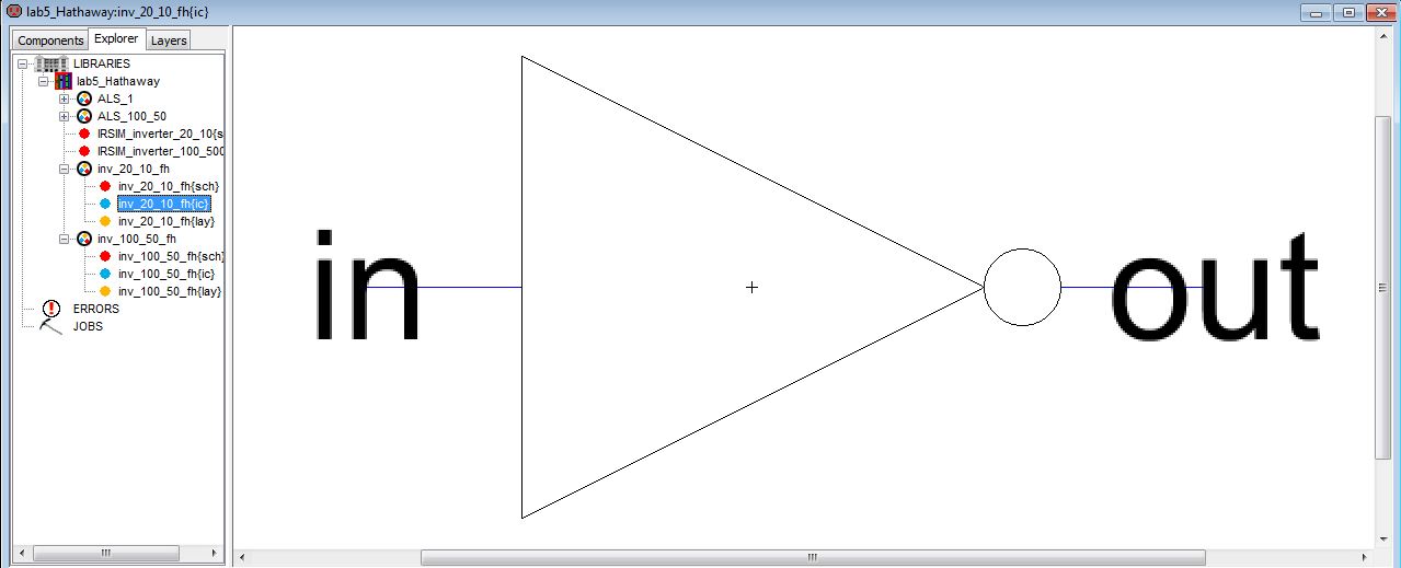
Icon view:
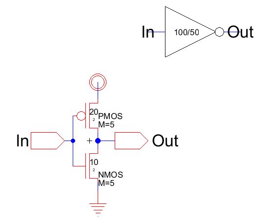
I
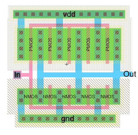
also created a PMOS with a width of 100, length 2 and a NMOS with a
width of 50 and length 2. Here instead of making a large version
of the transistor, I simply use the multiplier function in Electric.
Go to Tools->Simulation(Spice)->Add multiplier. This
will simulate having 5 transistors in parallel. Below is the
schematic with the icon that I created. Notice that the M=5 was
added to the PMOS and NMOS transistors.
The
next step is to create layouts of the above schematics. Once
again I followed the example in tutorial 3 for the layouts. When
exporting vdd and ground, make sure that they are in lower case.
Additionlly, make sure that your other exports match the
schematic exports or you will get errors. Once the layouts are
done, do a DRC, well check and NCC schematic layout view check (LVS).
Ensure there are no errors. Correct any errors that you may
have.
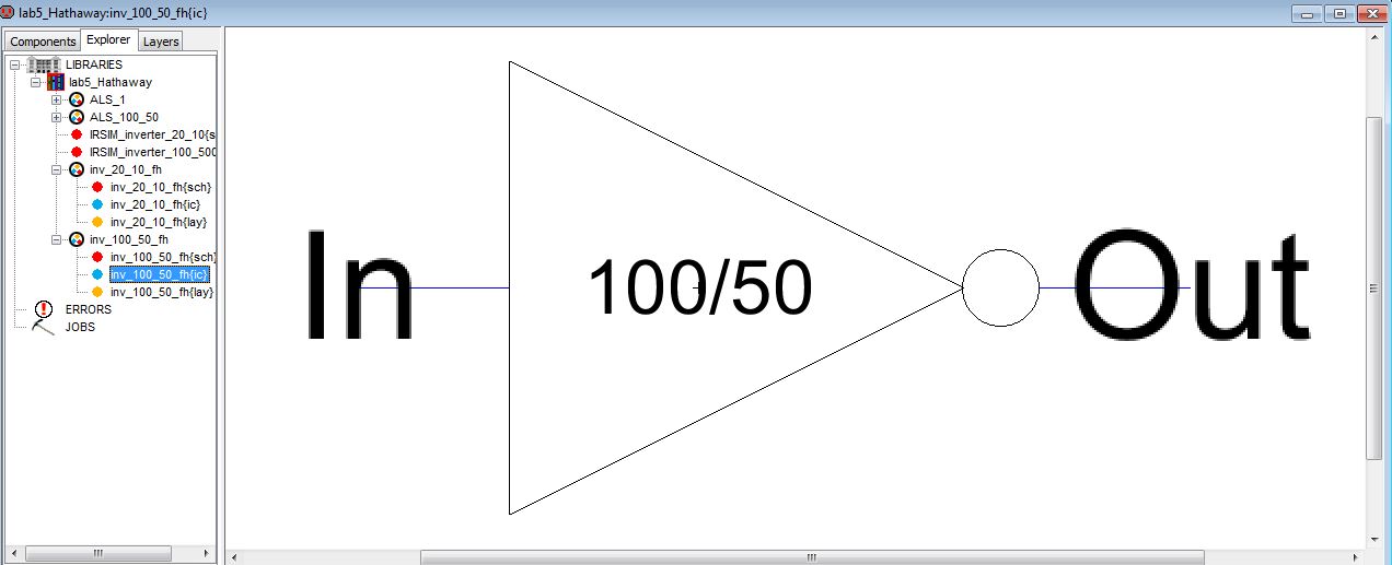
The layout of the 100/50 inverter:
Notice
that the nwell and pwell nodes are single row. We can do this to
save space. To create the 5 transistors in parallel, I simply
created 5 separate transistors and merged them together. Next
check for erros. I had several errors. To correct the
errors, I click Edit->cleanup cell->cleanup pin everywhere.
Additionally, I clicked on Tools->Routing->autostitch high
lighted now. This removed extra pins and overlapping connections.
Below is my layout. Notice vdd and gnd is lowercase and In and
Out exports match my schematic.
The
next step is to run the simulations. I will be using LTSpice, ALS
and IRSIM. The ALS simulator is built in to Electric but for the
IRSIM I had to download a file from here., Just follow the directions to install IRSIM.
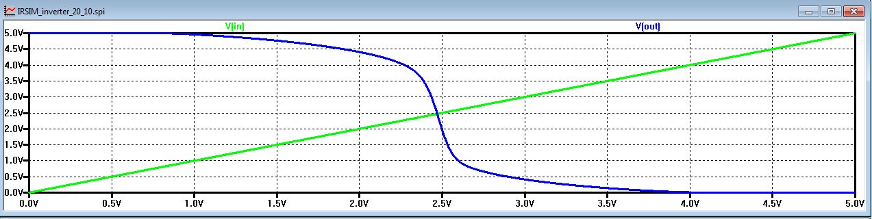
The LTSpice simulations were the same. Below is an example of the results.

All
of the LTSpice simulations were the same. It didn't matter what
capacitor load I used, the simulations results were the same.
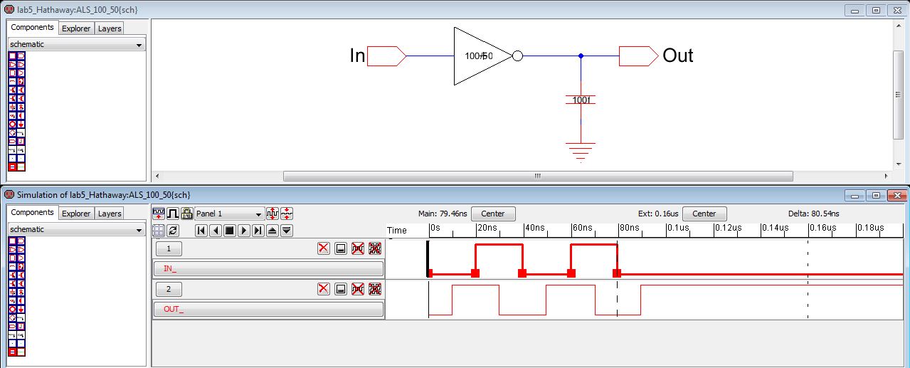
Below are my sims for ALS:
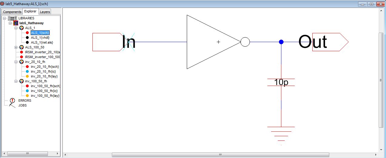
To
use ALS goto Tools->Simulation (built-in)->ALS:Simulate current
cell. I create a new schematic cell named ALS1 and used my icon
from the schematic created above and used this for my ALS sim:
Using
ALS for the first time was a little tricky. To set the signals I
backed the time hash marker (dotted line) back to zero. I pressed
G for a ground signal. You can also click Tools->Simulation
builtin->Set signal low at main time. Next I moved the time
marker out to the next time marked on the scale and pressed V or click
Tools->Simulation Built-in->set signal high at main time.
Below are my simuations.
100fF capacitor load:
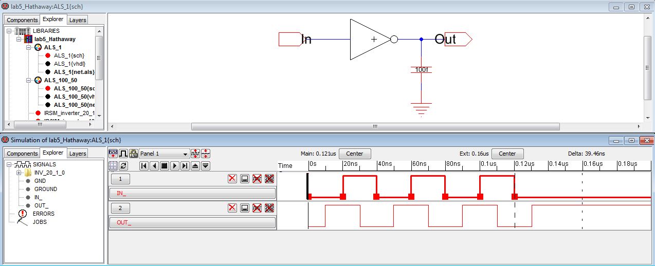
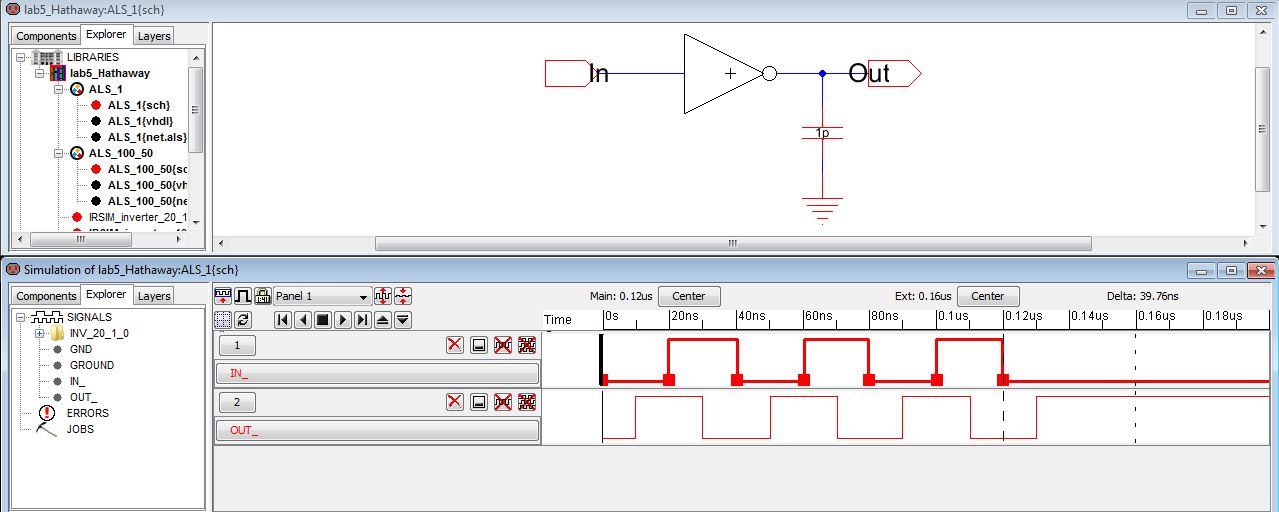
1pF capacitor load:
10pF capacitor load:
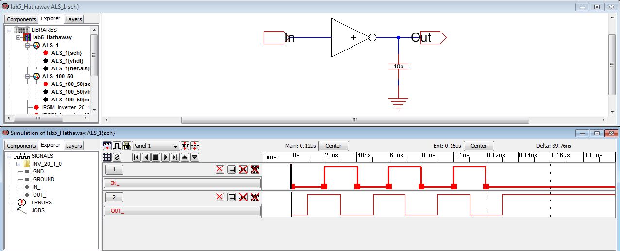
Notice
how the simulations are the same for the three simulations. ALS
doesn't simutate the transisitors very well, so the simulations are the
same for the three different loads.
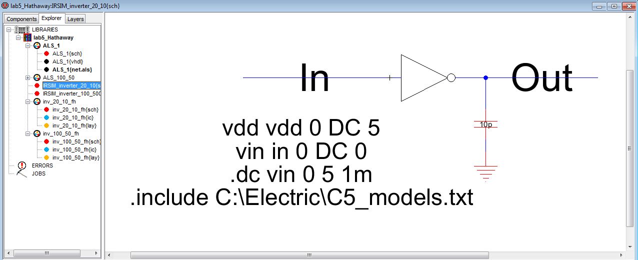
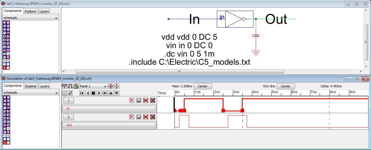
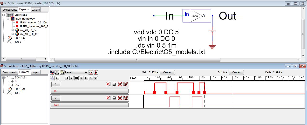
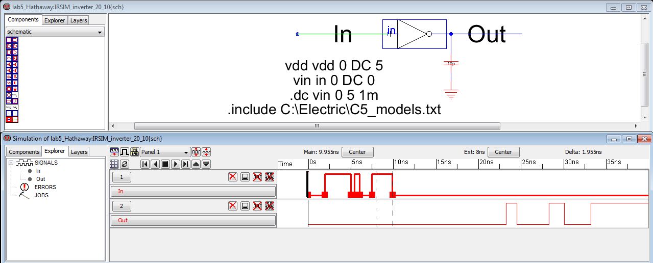
Below is the IRSIM simulations:
I created new simulation schematics for IRSIM:
Notice
that IRSIM does show the correct delays associated with the different
loads. IRSIM is accessed a similar way to ALS. Click on
Tool->Simulation Built_in->IRSIM simulate currect cell.
100fF capacitor load: We can see the delay.
1pF capacitor: Notice the delay.
10pF capacitor:
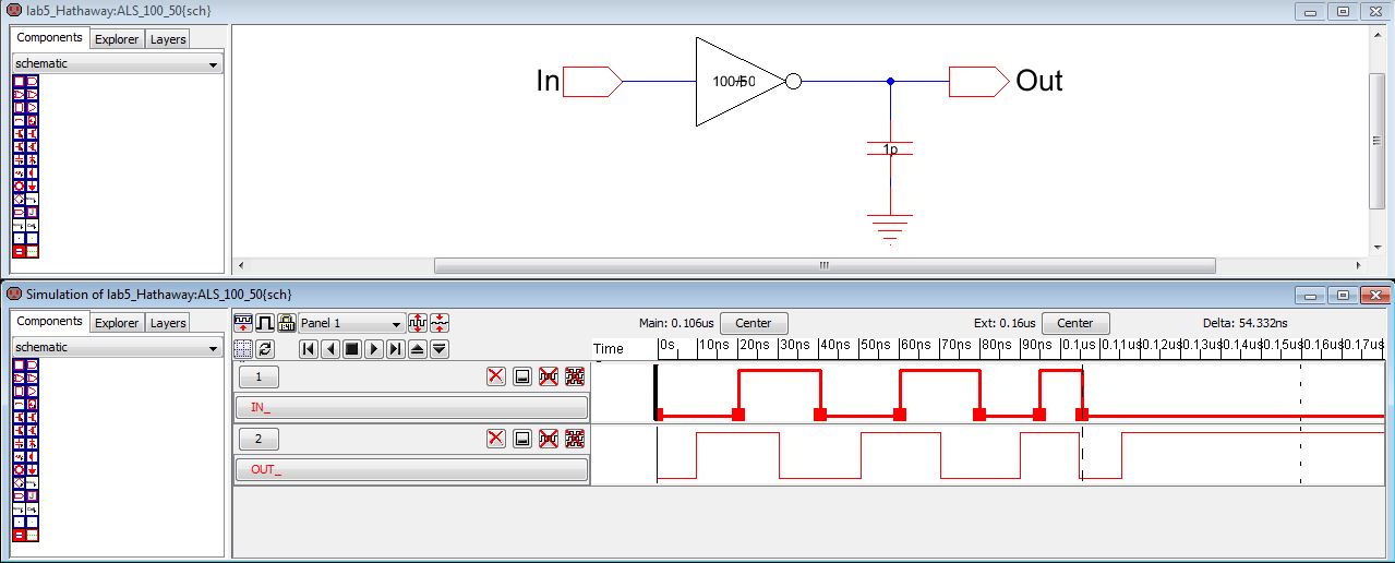
Next the simulations for the 100/50 inverter:
Again the LTSpice simulations were the same.
ALS simulations:
Notice that the delays are the same for the ALS simulations.
100fF:
1pF capacitor:

10pf capacitor:
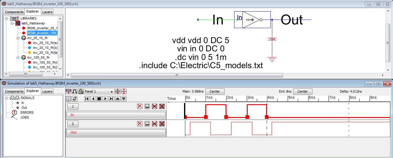
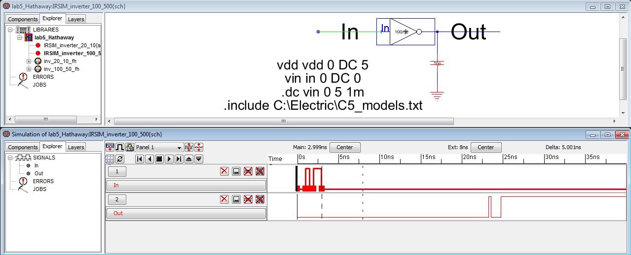
IRSIM of 100/50 inverter:
100fF capacitor load: Notice the delay.
1pF load: Again notice the delay. Now the delay has increased.
10pF load: Notice the increased delay with the 10pF cap.
We
saw above that ALS does simulate the logic, however, it doesn't
simulate the transistor level design. We can see that IRSIM did
model the transistors and we were able to see the delays with the three
different capacitor loads. This is very useful for us when we
design transistor circuits and we can model the circuits using electric
and verify our results. The conclusion for our results shows that
IRSIM is the best way to simulator our transistor level designs and
gives us the best results close to what we should expect.
I backed up my lab work by archiving directory, emailing and posting on the cmosedu website.
Copy of lab5_Hathaway.jelib file
Return to EE 421L Labs