Project - ECE 421L
This report covers the design, layout, and simulation of an 8 bit arithmetic logic unit with four function: logical AND, logical OR, addition, and subtraction.
The design is very modular, building heavily on the tutorials and previous labs.
The ALU:
Diagram Control Signals
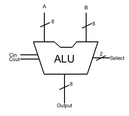
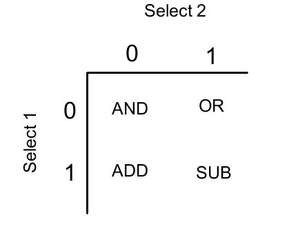
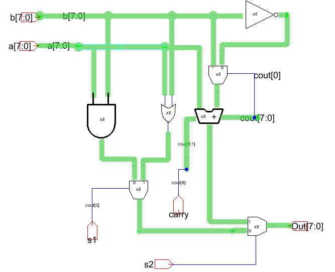
The ALU has 6 I/0 ports, containing two 8bit operands and corresponding 8bit output line, two 1bit selection pins, and carry functionality for arithmetic. The control signals for the ALU are depicted in the table. Lets look at the block-schematic for the ALU:
The design is modular, utilizing arrays of sub circuits connected with buses for a concise schematic.
We can break down each sub circuit individually for easier review.
Lets examine the individual logic gates, then review the 8bit adder.
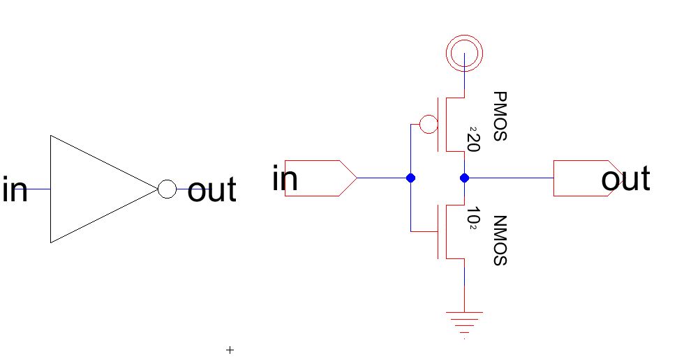
The Inverter
Here is the bottom level schematic of a single bit inverter. The 1bit inverter is placed into an array to create an 8bit inverter with buses to handle the I/O.
The length of the PMOS is designed to be twice the size of the NMOS for a symmetrical switching point.
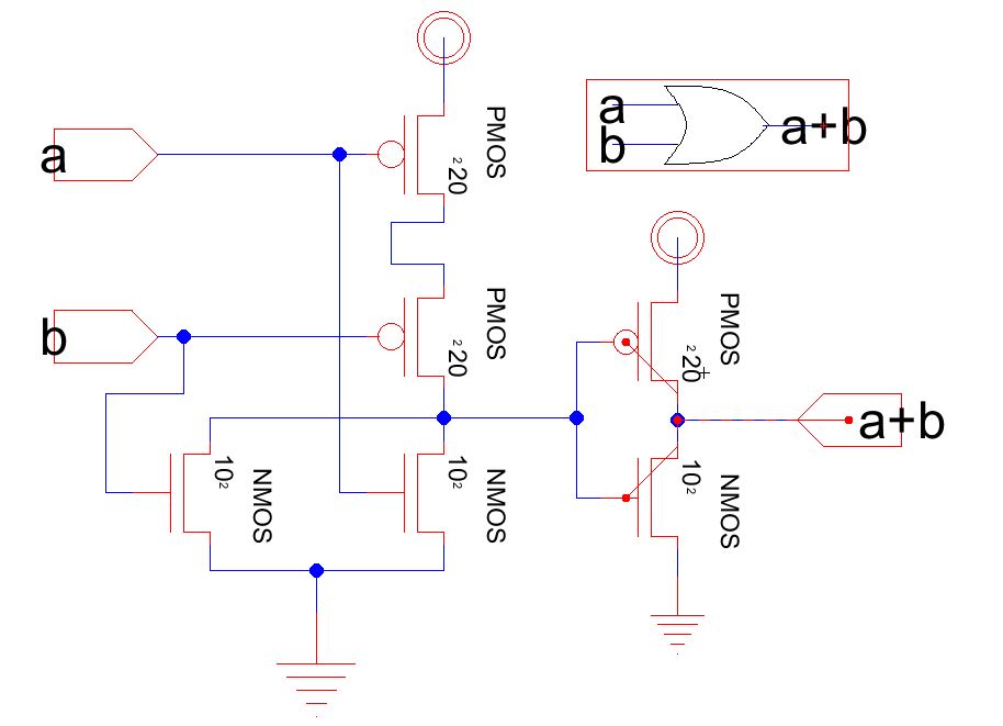
OR Gate
Here is the bottom level schematic of a two input logical OR gate. The 2 input gate is placed into an array to create an 8bit OR gate with buses to handle the I/O.
Construction of the OR logic is done by inverting the output of a logical NOR gate, and thus the OR gate also contains an inverter on the output.
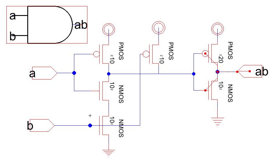
AND Gate
Here is the bottom level schematic of a two input logical AND gate. The 2 input gate is placed into an array to create an 8bit AND gate with buses to handle the I/O.
Construction of the AND logic is done by inverting the output of a logical NAND gate, and thus the AND gate also contains an inverter on the output.
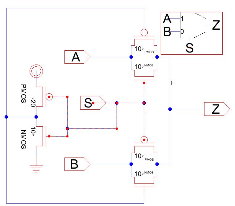
2 to 1 MUX
Here is the bottom level schematic of a two input the 2-to-1 MUX. The 2 input MUX is placed into an array and buses are used to create 8bit multiplexing; however, the level conversion is still 2 to 1, therefore each mux has a 1 bit selection pin for the multiplexing operation. Note that the multiplexer also includes an inverter for the selection pins.
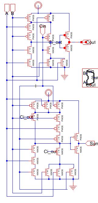
8bit Adder
The 8bit adder is a ripple carry adder based off of Fig. 12.20 of the CMOS text. Each adder is arrayed and buses are used for the IO. Note the connection label for the carry flags on the adder: the Cin array runs from [7:0] and the Cout array runs from [8:1], meaning lines [7:1] are connected. In the ripple-carry design, there is 1 carry in and carry out for the full adder as a whole, and the intermediate carry flags are tied together (hence "ripple carry").
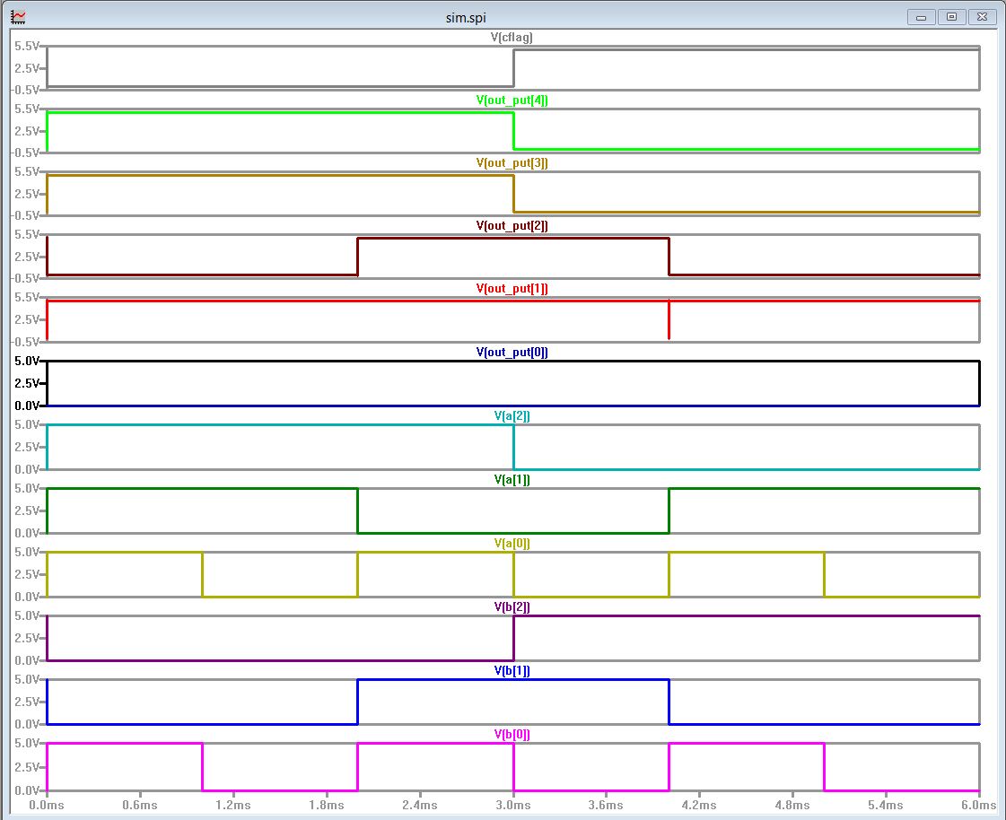
Simulations
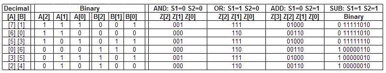
Lets verify the functionality of the ALU with LT Spice. We will use the following truth table for verification. Here only the first two bits are sample with all possible outputs, and a few random choices are added to test the rest of the functionality. Obviously, we do not want to manually test all 2^8 combinations for accuracy.
Logical AND Simulation
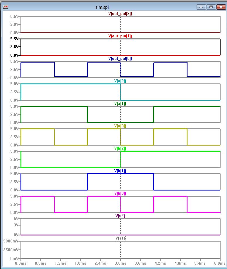
Logical OR simulation
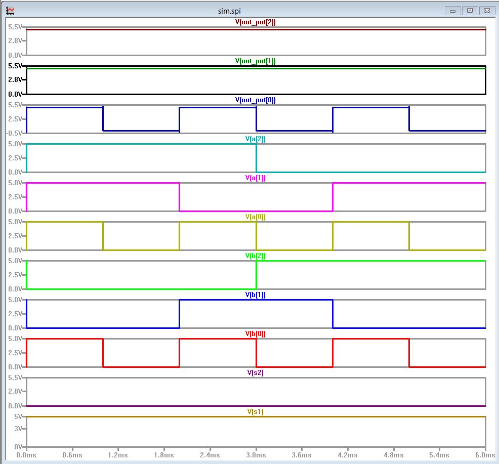
Addition simulation
SUB
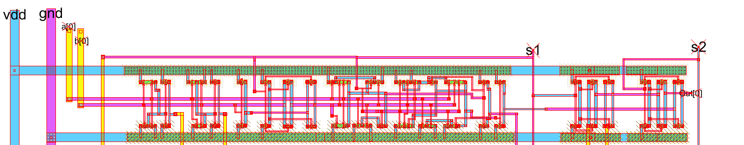
The simulation of our schematic is correct, so we can move on to the layout of the ALU. For the layout, it makes sense to layout a 1 bit ALU and cascade them together to form the 8bit device.This will make for a nice modular design. Lets start with the logic gates, and then move on to the adder/subtracter.
OR GATE AND GATE NOT GATE
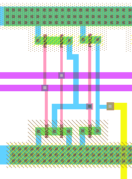
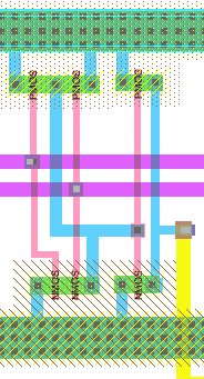
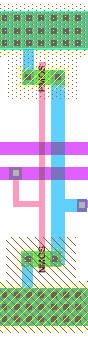
The layout logic gates should be formilar from previous labs. Each gate is 2 or 1 input and will be cascaded to make the 8bit logic.
The layout of the MUX is straight froward using figure 13.6 from the text:
2-1 MUX
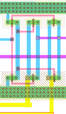
By combining the above layouts, we can form the 1 bit ALU:
Cascading 8 1bit ALUs make up the 8bit ALU layout
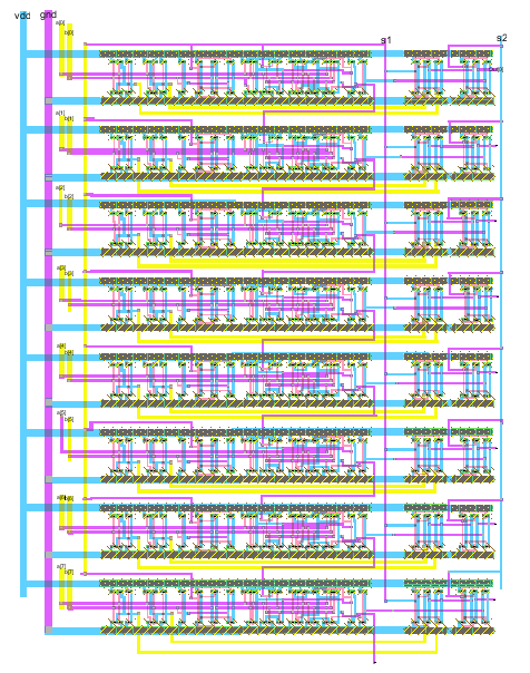
The layout passes DRC, LVS, and Well Check.
Backups:
