
Lab 7- ECE 421L
Using buses and arrays in the design of word inverters, muxes, and high-speed adders
Go through tutorial 5 and learn how to create arrays and busses.
For this lab, we will be converting the 1 bit INV, NAND, AND, OR, NOR gates to 8bit logic gates.
Lets start with the 1bit inverter. Turn the inverter into an 8bit array as in tutorial 5. Then export the input and output via busses as shown.
Next, create an icon view of the cell as we will use it for simulation. Using the schematics from previous labs, continue and create the 8-bit NAND, NOR, AND, and OR gates.
1. INVERTER
Before continuing, lets examin the simulation of the inverter driving a few capacitors:


Notice how out[2] can't fully drive the 1pF capacitor.
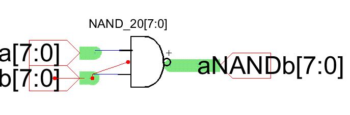
Continue and create the 8bit busses of the remain logic gates as shown:
2. NAND
3. AND

4. NOR

5. OR

Next, we will simulate the output of each gate on a single schematic:


We have built all the parts required to implement a full adder. We will build a full adder from transistor level.


Backups:
