

Lab 4 - ECE 421L
For this lab, will will need the C5 models. Save C5_models.txt to your working directory
We will begin by creating to schematics for our transistors. Create two new cells: NMOS_IV{sch} and PMOS_IV{sch}. Starting with the NMOS schematic, place an NMOS transistor down and export (ctrl+e) the source, gate, and drain as shown. Furthermore, change the width (ctrl-i) of the NMOS and PMOS transistors to 10 and 20 respectivly.
Next, set the spice models (Tools -> Spice -> set spice model) of the transistors to NMOS and PMOS.
Notice the hanging VDD and GND symbols on each schematic. We must include these so that our schematic will match our layout, as we are using three terminal pins in our schematics. Our layout will still include the bulk, but it will be tied to gnd or vdd.
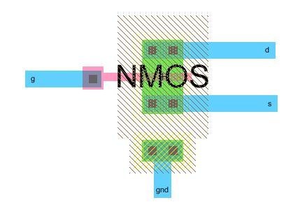
Next, we will create the layout for our two schematics. Create two new cells: NMOS_IV{lay} and PMOS_IV{lay}. Starting with the NMOS, lay down the following components:

As done in Tutorial 2, make the adjustments to each component as necessary to match the schematic. Most importantly, change the width of each component to 10/20 (NMOS/PMOS) and rename the NMOS spice model to "NMOS".
Connect the components to form the transistor, as in tutorial 2:
Do the same for the pmos (that is, follow tutorial 2):
Using the following components

We can connect together our pmos device:

We should now have a schematic and layout for both our NMOS and PMOS device in our library. Remember that detailed instructions for building the layout is in Tutorial 2, linked at the top of the page. Make sure your layout and schematic pass DRC, well check, and layout-vs-schematic. We are ready to simulate our transistor's IV characteristics.
To do so, we are going to create 2 simulation cells (NMOS_SIM / PMOS_SIM or similar). With these cells, we will create icons for our transistors and add the spice code for simulation.
Create a two new cells for simulation and add the transistors and the following spice code:


Next we want to create an icon for each: View -> make icon view
Draw the NMOS and PMOS icons using the artwork components. To make lines, place black circles on the canvas and connect the dots.
Arrange the pins appropriately.
![]()
![]()
Finally, use the icons and simulate the IV characteristics of the transistors.


Finally, back up your work:
