Project Report - ECE 420L
Lab Report
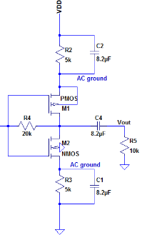
A push-pull amplifier can be used as a transimpedance amplifier, since it has high gain, and can drive a load since it can also act as a buffer.
The gain of a transimpedance amplifier is the voltage out divided by the current in (Vout/IIN). The capacitors are added to ensure we can treat the sources as AC ground, for the gain analysis.
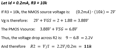
We know the values of KP and threshold voltage from the Spice model (see Lab 6 ) for the ZVN3306A and ZVP3306A MOSFETs. From there, we can set the drain current to a value under .3mA, and solve for the VGS, VSG, and the resistor values, after fixing one resistor value (say, R3 in the schematic above).
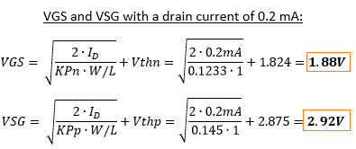
Calculations:
KPn = 0.1233 Vthn = 1.824V
KPp = 0.145 Vthp = 2.875V
Using a value of 10k for the resistors connected to the sources of the MOSFETs will limit the current drawn by the circuit.
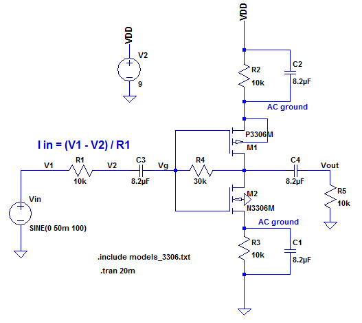
The final schematic is shown here:
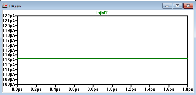
The current through the circuit, with the input disconnected (the wire cut between C3 and Vg) is simulated to make sure it is near under .2mA as intended:
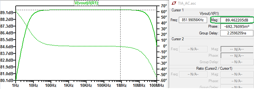
A gain of 30,000 is equal to 20log(30,000) = 89.5 dB. Simulating the frequency response of the circuit, a 30k resistor value for R4 was found to create an overall gain of 89 dB :
Transient Simulation:
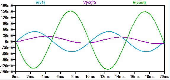
(Note: V(v2) is multiplied by 5 so that it's value can be read more easily from the waveform.)
The gain can be estimated as160mV/ (60mV-6mV/ 10k ) = 160m/5.4u = 29.6 k.
Measured gain at 100 Hz:
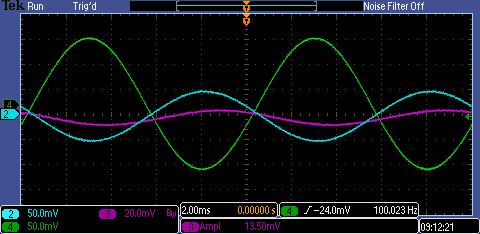
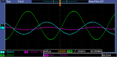
The blue wave, Channel 2, is the input signal, amplitude 50mV. The purple wave (channel 3) is the signal across the 10k input resistor, with an amplitude of 11 to 13mV (11mV was used in the calculation seen below, but 13mV was also seen, as in the oscilloscope screenshot above).
The green wave (Channel 4) is the output voltage of the push-pull TIA.
The calculations for the gain of the circuit from the measured results is shown here:
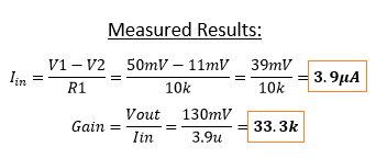
Thus, an input current of 3.9 uA is converted to an output voltage of 125mV peak-to-peak at 100Hz. (The speed of the amplifier is determined below; the design operates with the same gain up to about 60kHz.)
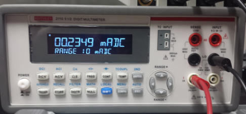
The amplifier is drawing 235 uA from the power supply:
Maximum Output Swing:
The output swing was found by increasing the amplitude of the input voltage (and consequently the input current) and looking at the waveforem when the output was clipped to its maximum and minumum values:
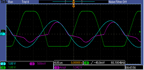
The output swing of this design is from about 4.5 V. This output swing may be able to increase with added PMOS and NMOS devices in parallel, with larger resistors to account for the greater current demand.
In conclusion, this lab has presented how the push-pull amplifier can be implemented as a transimpedance amplifier drawing very little current but working effectively at taking a small input current, and amplifying the signal to a readable output voltage.