Lab 6 - ECE 420L
The report is split up into four parts, detailing the theory and operation of each of the following four amplifier configurations:
Part 1: Source Follower (Common Drain) amplifiers
Part 2: Common Source amplifiers
Part 3: Common Gate amplifiers
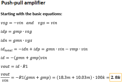
Part 4: Push-Pull amplifier
Each part should include:
Lab Report
Part 1: Common Drain (Source Follower) amplifier
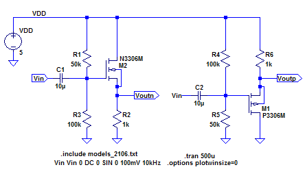
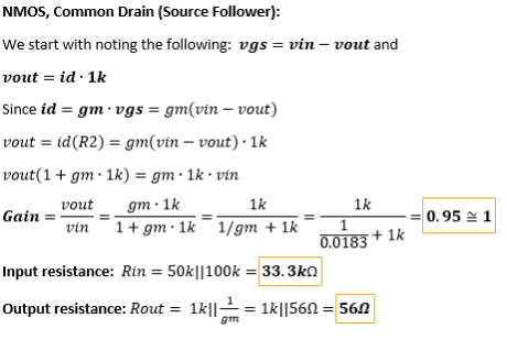
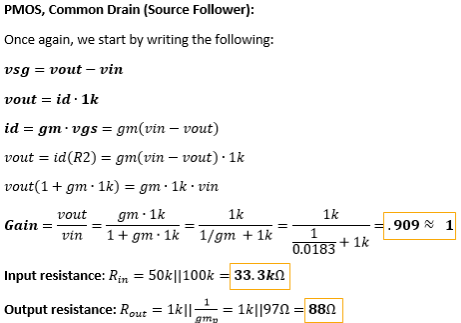
The common drain amplifier is called a source follower, because the gain of these amplifiers is one. They have a fairly high input resistance as we will see in the calculations, and a relatively low output resistance. The drain of each MOSFET is common to the input and output, thus the name Common Drain. The common drain amplifier circuit (both NMOS and PMOS) is shown below:
A note about electrolytic capacitors:
Electrolytic
capacitors were used for building the circuits in this lab. The '+' terminal of
the elctrolytic capacitor should be connected to the higher DC voltage,
so that a reverse chemical reaction does not occur inside the
capacitor, which would result in a breakdown of the thin dielectric
insulation layer separating the plates of the capacitor, thus ruining
the capacitor.
To
analyze this amplifier, we will begin by finding the DC bias, or
operating point. For the calculations, the KP and W/L values were found
in the LTSpice ZVP/N3306 models used in lab6_sims.zip .
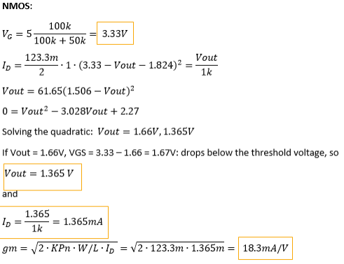
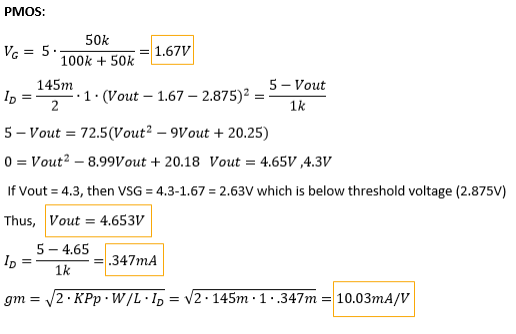
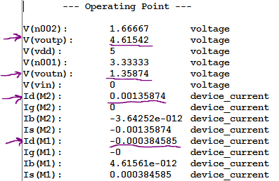
DC operating point calculations:
The DC operating point and calculated gm can be comfirmed in LTSpice using the .op simulation and viewing the Error log, respectively:
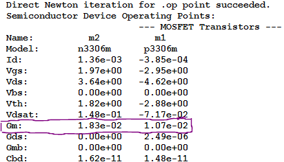
Hand calculations for gain and input and output resistances are as follows:
Simulation of Common Drain amplifier gain:
To measure the input and output resistance in simulations, we simply find the current going in or out, and divide the input or output voltage by that current.
Simulation of Common Drain input resistance, for NMOS and PMOS:
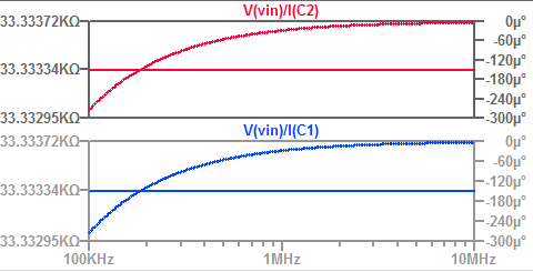
We need to determine the input and output resistance differently in the lab, since we do not have current probes.
To measure the input resistance, we do the following:
- Connect a resistor with the value of the input resistance calculated by hand in series before the input capacitor (which protects the DC bias).
- Measure the voltage at the input of the capacitor
- Since the added resistor creates a voltage divider with the input resistance, if the input resistance is close to what was calculated by hand, the voltage should drop by half across the resistor.
- If the voltage is not exactly half, we can use the voltage divider equation to solve for the input resistance.
To measure the output resistance, a similar procedure is followed:
- Connect a resistor in parallel with the output resistor, with an added big capacitor (which will act as a short for AC but an open for DC) so that the DC bias is not altered.
- The output of the amplifier is then expected to be half of its previous value
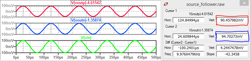
Experimental results for the NMOS Common Drain (Source Follower):
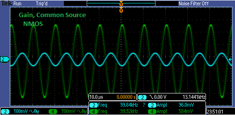
Note: In the oscilloscope screenshots, the outputs are always the green waveform (channel 4), and the inputs are blue (channel 2).
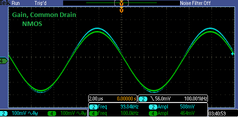
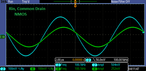
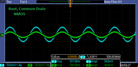
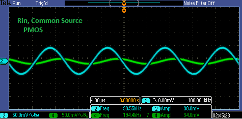
From the gain waveform, we can calculate the gain by finding Vout/Vin = 464mV/508mV = 0.91, Rin and Rout can be confirmed at 33k and 56 Ohms, respectively, since the output waveforms are half of the input waveforms, roughly.
Experimental results for the PMOS Common Drain (Source Follower):
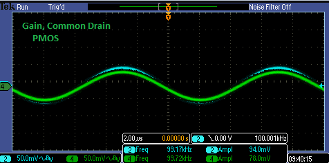
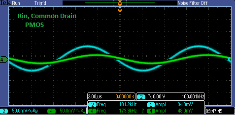
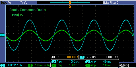
Table summarizing theoretical and experimental results:
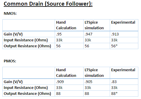
* The experimentally determined values for the resistors are approximately correct, verified experimentally. Solving the voltage divider Vin = Vout (Rin/(Rin+33k) will give an equation for the actual Rin: Rin = 33k*Vin/(Vout-Vin) where Vin is the input, Vout is the voltage that we expect to be half of the input if the actual Rin is 33k ohms. Since the experiment yielded good enough results to confirm the input and output resistances, the Experimnetal value of 33k and 88 ohms was kept for Rin and Rout, respectively. This approximation will be continued for the other amplifiers as well.
Part 2: Common Source Amplifiers
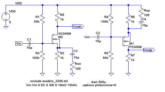
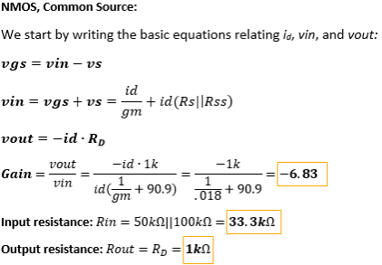
Hand calculations for the gain, input resistance, and output resistance:
Simulations:
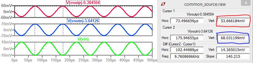
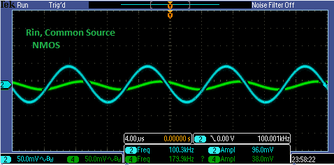
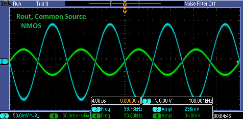
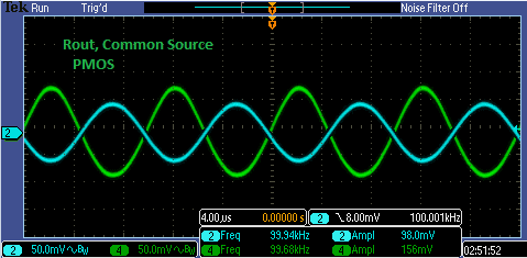
Experimental results for Common Source gain, input resistance, and output resistance:
The gains for the Common Source determined experimentally were not as good as expected from the simulations and hand calculations. Some transistors even gave lower gains than the gain seen above.
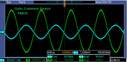
For example, for the PMOS circuit, I switched out the transistor while leaving everything else in the circuit totally unchanged. The gain was terrible closer to one than 5 or 6, the gain we expect:
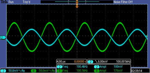
After this was discovered, multiple transistors were tried if the gain was very different from what was expected. However, the gain of around 3 for the PMOS Common Source circuit was the best that was achieved.
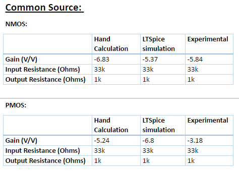
Table summarizing Common Source experiments:
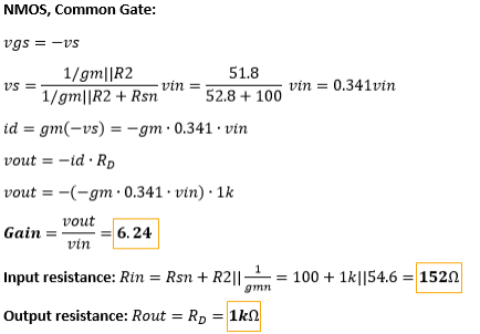
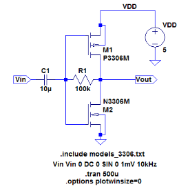
Part 3: Common Gate Amplifiers
The gate of the transistor is common to the input and output in this topology.
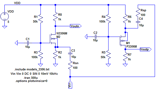
Hand Calculations for gain, input resistance, and output resistance
:
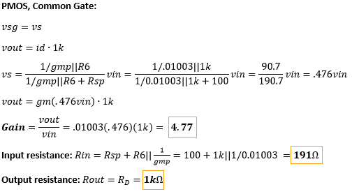
LTSpice Simulation:
Experimental results:
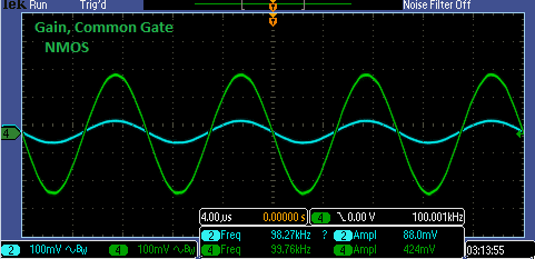
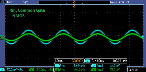
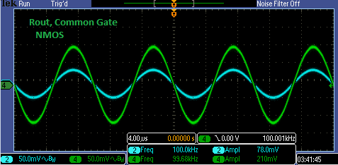
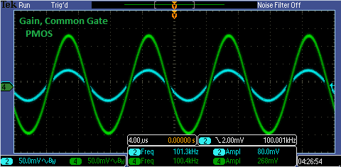
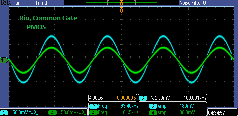
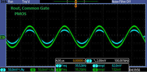
Table summarizing experimental vs. theoretical values:
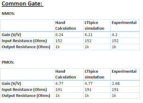
Experimentally verifying this amplifier proved to be challenging.
The following oscilloscope screenshot shows the best gain I was able to see, only about 600, where the calculation and simulations show that the gain should be nearly 3000.
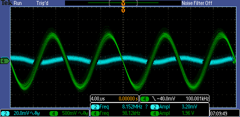
The gain is 1.96V/3.2mV = 612.5 V/V.