Lab 5 - ECE 420L
Authored
by Stephanie Silic
silics@unlv.nevada.edu
March 8th, 2017
Lab Description
This lab covers the op-amp integrator and its frequency response and how to use the integrator to generate a triangle wave.
Lab Report
This lab will again utilize the LM324 op-amp (LM324.pdf).
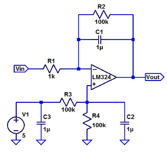
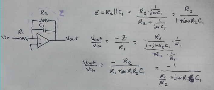
- Calculate the frequency response of the following circuit. Ensure you show your clear hand calculations.
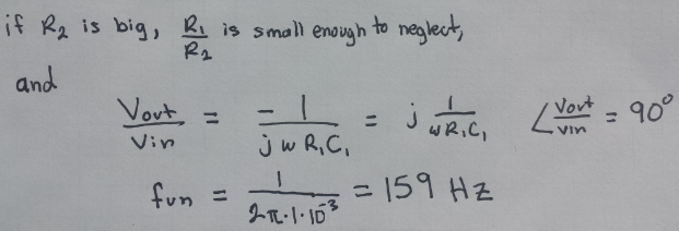
- What can you neglect to simplify the calculation?
The 100k resistor can be neglected to simplify the calculation, as shown below:
- Does the circuit work if you remove the 100k? Why or why not?
The
actual circuit will not work if we remove the big resistor in the
feedback loop because it will affect the DC offset too much and the
signal will likely clip at one of the rails.
- Does the 100k have much of an effect on the frequency response?
We
can see from the transfer function calculations shown above that the
100k resistor does not have much effect on the frequency response.
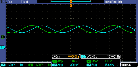
- Verify calculations with experimental results.
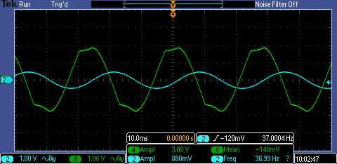
- Show that the input and output of the integrator
have the same peak values at the unity gain frequency.
The oscilloscope screenshot below shows the input in blue (channel 2) and the output in green (channel 4):
Note: the Mean
measurement for the output shows that it is centered around 1.08, I had
adjusted the DC offset of the input waveform which shifted the output
down.
Decreasing the frequency gives a higher gain, until we start to hit the rails of the op-amp (see Lab 3)
- Is the phase shift between the input and the output what you expect? Why or why not?
The phase shift we expect is Vout leading Vin by 90 degrees.
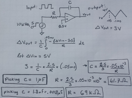
- Next, design, simulate, and build a square-wave to triangle wave generation circuit.
- Assume the input/output frequency is 10kHz and the output ramp must swing from 1 to 4V centered around 2.5V.
- Show all calculations and discuss the trade-offs (capacitor and resistor values, input peak, min, and average, etc.)
Hand calculations for the triangle wave generator:
The most obvious tradeoff we can see that a smaller capacitor value will result in a bigger resistor value. Also, as the peak input value goes up, the resistor value will need to be bigger.
With
the larger capacitor size, there seemed to be worse results. This is
probably due to human error. However, I chose a smaller capacitor and
larger resistor to compare the results and got a better triangle
wave.
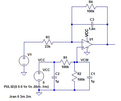
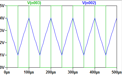
LTSpice circuit and simulation of the design:
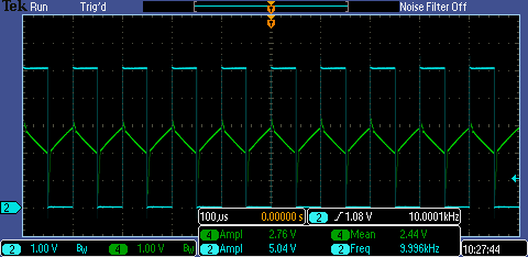
Oscilloscope measurements from the circuit (C = 1.8nF, R = 69kOhm):
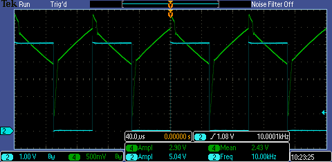
Zooming in on a couple periods of the output reveals undesired spikes in the waveform:
(note: the output waveform is also at a smaller scale factor, 500mV in the screenshot below.)
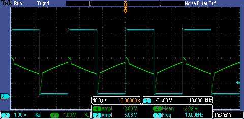
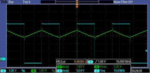
Adjusting the DC offset gave the following results:
Lower
DC offset:
Higher DC offset:
Return to my labs