Lab 3 - ECE 420L
Authored
by Stephanie Silic
silics@unlv.nevada.edu
February 10th, 2017
Lab Description
This lab will utilize the LM324 op-amp (LM324.pdf) and a few other op-amps to compare their offset voltages.
We will analyze basic topologies, finite gain, and offset.
Support answers with the datasheets referenced, hand calculations, LTspice simulations, and experimantal results.
My report includes the following sections:
- Part 1: LM324 Datasheet Questions
- Part 2: Analysis of basic op-amp operation
- Part 3: Measurement of 4 op-amp offset voltages
Lab Report
Part 1 - LM324 Datasheet Questions:
- Knowing
the non-inverting input, Vp, is at the same potential as the inverting
input, Vm, (called the common-mode voltage, VCM) what are the maximum
and minimum allowable common-mode voltages? Support your answer with an entry from the electrical characteristics table in the datasheet.
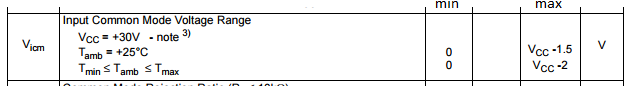
As seen below, at ambient temperature (25 degrees Celcius), the
Common Mode Voltage range is from 0V minimum to (Vcc - 1.5V) maximum,
which, if Vcc is 5 - 1.5 = 3.5V .
- What is a good estimate for the op-amp's open-loop gain? Support your answer with a plot from the datasheet and an entry from the electrical characteristics table.
The open-loop gain of the op-amp is also referred to in general as the op-amp gain, and is usually represented by the notation AOL. The gain of the op-amp can be found from the open loop frequency response of the op-amp, shown below (left):
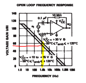
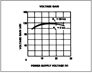
Looking
at the frequency response plot, the open-loop gain at 1kHz is about
60dB, or 1000. ( dB = 20log(x) ). From the other plots, we can see that
the gain does not change much with temperature or power supply voltage,
so we can estimate AOL = 1000 at 1kHz.
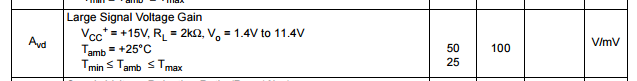
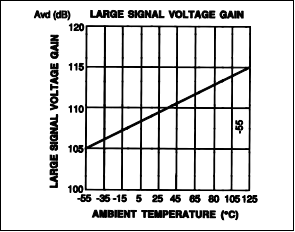
The large signal voltage gain at room temperature (25 degrees Celcius)
can be read from the plot shown above as about 100dB
The entry for large signal gain in the Electrical Characteristics Table
also tells us that the gain i 100V/mV, which is 100x10^3 V/V, or 100dB,
at room temperature:
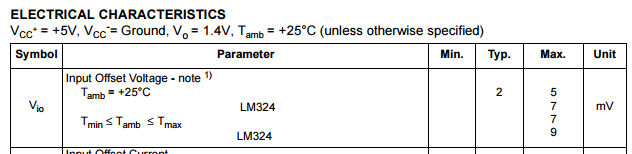
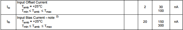
- What is a good estimate for the offset voltage?
At room temperature, the offset of this op-amp should be 2mV, according to the datasheet:
- For worst case design what value would you use?
Since the maximum input offset voltage is 7 to 9 mV, I would assume a 9mV offset as a worst case design value.
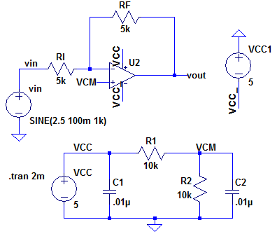
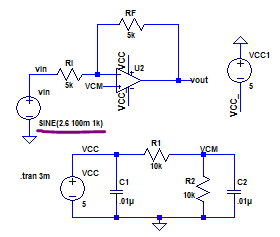
Part 2 - Build and test the following op-amp circuit:
- What is the common-mode voltage, VCM? Does VCM change? Why or why not?
The common-mode voltage is the voltage seen at the input terminals of
the op amp. In this circuit, it is 2.5V, created by the voltage divider
circuit built with two 10k resistors. The capacitors seen in the
voltage divider circuit are treated as open circuits since we are
operating with DC conditions. - What is the ideal closed-loop gain?
The ideal closed-loop gain is
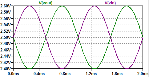
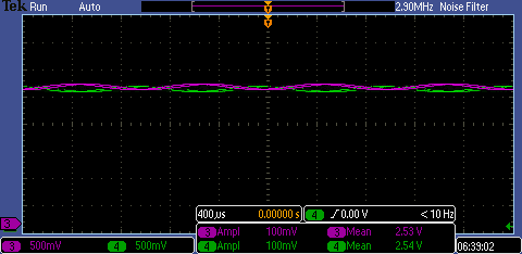
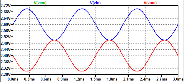
the gain of the op-amp in the inverting configuration, which is -RF/RI , or -1. Thus, the output will have a gain of 1 and 180 degrees out of phase with the input. - What is the output swing and what is it centered around? What happens if the input isn't centered around VCM, that is, 2.5V? Provide a detailed discussion illustrating that you understand what is going on.
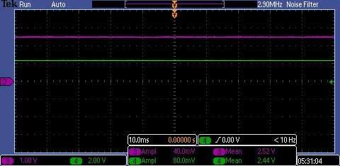
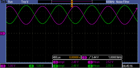
- The output swing is
the 100mV signal which "swings" around the DC offset of 2.5V.
That is, the signal varies from 100mV above and 100mV below the 2.5V,
or 100mV centered around 2.5V. This is shown below in the simulation
and oscilloscope measurement of the op-amp circuit:
LTSpice simulation of the circuit:
Oscilloscope screenshot:
- What is the maximum allowable input signal amplitude? Why?
-
The maximum allowable input signal amplitude is 2.5V. This is because
the output of an op amp is limited by the supply rails, +Vcc and -Vcc.
For us, +Vcc is 5V and -Vcc is 0V. Thus, for our signal centered at
2.5V and with a gain of 1, the input signal amplitude should be limited
to 2.5V. Anything above that would exceed the 0 to 5V rails.
Input at 2.5V, the input limit:
 Input at ~3.8V, causing clipping (output on channel 4, green):
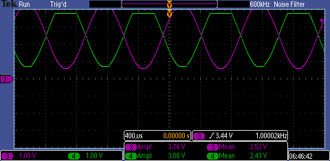
- What is the maximum allowable input signal if the magnitude of the gain is increased to 10? Why?
-
If we have a gain of 10 instead of 1, the output will be the same at 1/10th the input. Therefore the maximum allowable input signal should be .1(2.5V) = 250mV.
- What
is the point of the 0.01 uF capacitors from VCC and VCM to ground? Are
these values critical or could 0.1 uF, 1000 pF, 1 uF, etc. capacitors
be used?
- The
capacitors are there to store charge as decoupling capacitors to help
the voltage divider to stay at a consistent value and reduce the impact
of noise. Their size is not critical. The capacitors do not effect the DC voltage divider. - The datasheet
shows that this op-amp has an input bias current that flows out of the
op-amp's inputs of typically 20nA. This current flows out of both the
non-inverting and inverting inputs through the resistors connected to
these inputs. Show how the operation of the circuit can be effected if,
for example, R1 and R2 are much larger.
-
As stated above, the op-amp has an input bias current flowing out of
its terminals of 20nA. If the resistor values are in the Gigaohm and
higher range, the 20nA flowing through Gigaohm resistor values will
cause Volts of change. If this
happens,
the signal will no longer be centered at VCM as it should be, and we
may get clipping or worse. - What is the input offset current? What does this term describe?
- The input offset current, IOS, is the difference between the input bias currents at the teminals of the op amp. That is, IOS = (IB+ - IB-). According
to the datasheet of the LM324, its input bias currents are typically
20nA and the input offset current is typically 2nA:
Part 3: Measurement of 4 different op-amp offset voltages:
- Explain how the following circuit can be used to measure the op-amp's offset voltage.
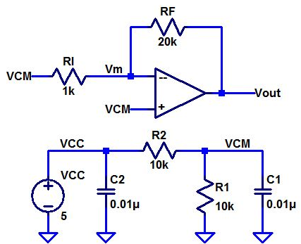
In the circuit shown above, VCM is the input to both terminals of the op-amp. We remember two important things:
1) The op amp tries to keep Vm equal to Vp (which is VCM).
2) The potential across RI
would be zero if Vm was exactly equal to VCM and from KCL, zero
current would flow through the feedback resistor also. Thus VCM - Vout
= 0 or Vout = VCM.
Since
the op amp may not be able to get Vm exactly equal to VCM, the
potential at Vm will be VCM plus a small offset voltage. This offset
voltage at Vm will be amplified by RF/RI or 20, using the resistor
values seen above. If a 100k ohm resistor is used in place of the 20k
ohm resistor, the offset voltage will be amplified by 100. Some hand calculations supporting this discussion are shown below:
Therefore,
to calculate the offset, the difference between Vout and VCM is
measured, and the offset voltage will be this difference divided by the
20 or 100 depending on which resistor values are used.
Finally, we find the offset voltages of 4 different op-amps, including the LM324 used in part 2.
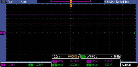
LM324 Offset voltage measurement and calculations:
Offset voltage = (VCM-Vout)/20 = 2.54 - 2.44/20 = 5.0mV
This measured value is above the 2mV typical value and below the 9mV worst case value seen in the datasheet.
LM339 Offset voltage measurement and calculations, and comparison to datasheet:
Offset voltage = (VCM-Vout)/20 = 2.54-2.52/20 = 1.0mV 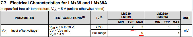
LM348 Offset voltage measurement and calculations and comparison to datasheet:
Offset voltage = (VCM-Vout)/10 = 2.55-2.6/20= 2.5mV 
LM393 Offset measurement and calculations:
Offset voltage = (VCM-Vout)/20 =2.54-2.52/20 = 1.0mV 
All work backed up:

Return to my labs