Lab 1 - ECE 420L
For
this first lab simulate, and verify the simulation results with
experimental measurements, the circuits seen in Figs. 1.21, 1.22, and
1.24 (use a 1 uF cap in place of the 1 pF cap) of the book.
Your results should be similar to, but more complete than, the
simulation results seen on pages 17 - 23. In your report, and for
each circuit, show the
For
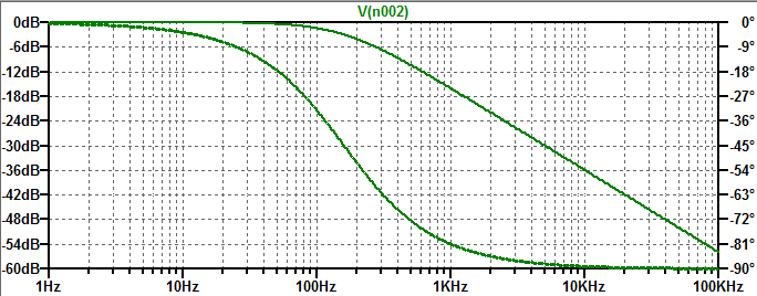
the AC response seen in Fig. 1.23 generate a table showing some
representative measurement results (frequency, magnitude, and
phase).
If you would like to include a plot of this measured data then using a plotting program, such as Excel, add the image to your report.
Lab Report
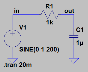
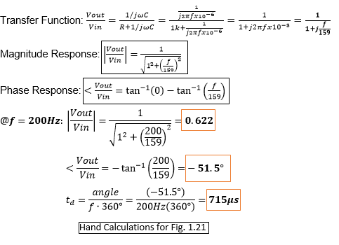
Part 1 - Analysis of Fig. 1.21
The negative sign for the phase of Vout/Vin indicates that Vout is lagging Vin.
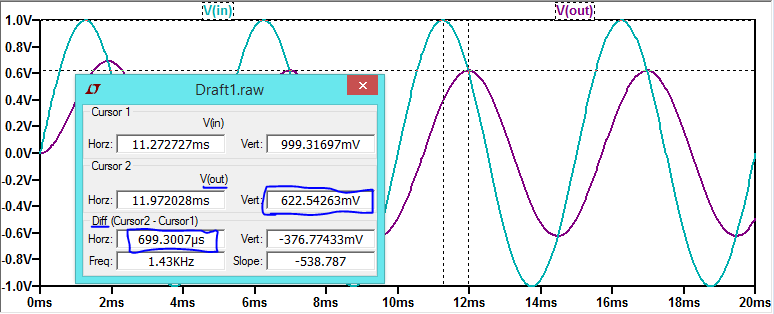
LTSpice simulations; transient and AC analysis:
Transient analysis (.tran 20m):
Experimental measurements:
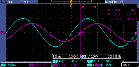
Note: Channel 3 has a V/division scale of 50mV/division. This is because I was using an oscilloscope probe set to 1X on the output waveform while the input waveform was probed with a 10X probe. This simply means I have to multiply the values read on this channel by 10. Thus, the 62.0mV peak value of the output waveform is actually 620.0mV.
The magnitude and phase is found from the oscilloscope as shown above; the values in a frequency range from 1Hz to 100kHz are shown in the following table:
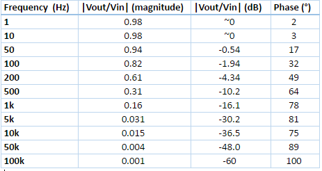
From this table of experimental values, we can match them to the Bode plot generated with LTSpice earlier. The higher frequencies were difficult to accurately measure on the oscilloscope, so the phase at 100kHz is not really expected to be 100 degrees. At 200 Hz, the frequency at which the simulation and hand calculations were made, the phase is about 49 degrees and the magnitude is about -4.34dB, or 0.607. ( xdB=20log(x) ).
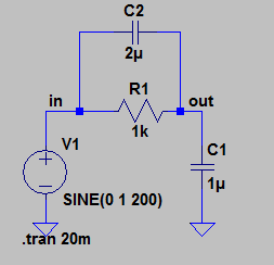
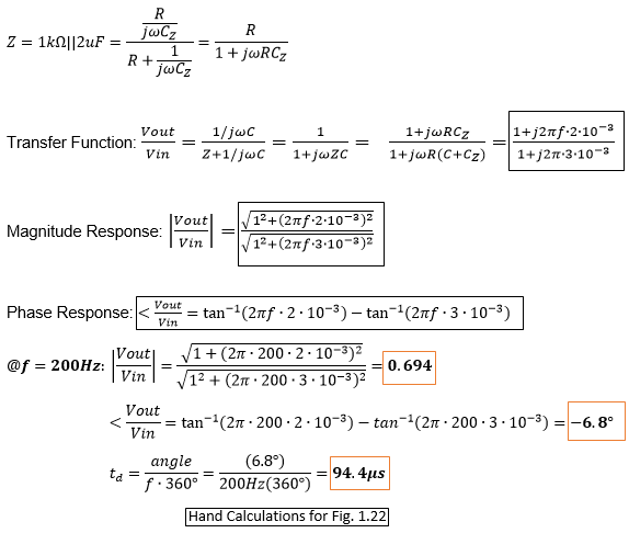
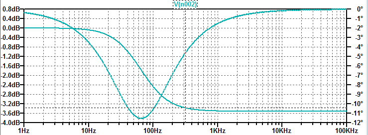
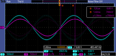
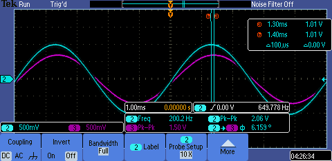
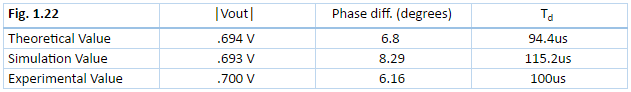
Part 2 - Analysis of Fig 1.22
Circuit and hand calculations of theoretical values:
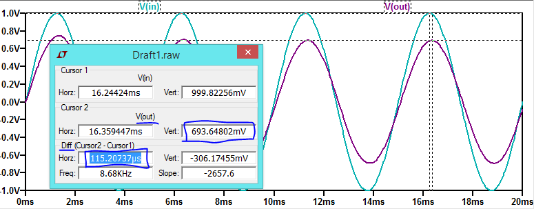
Simulation in LTSpice:
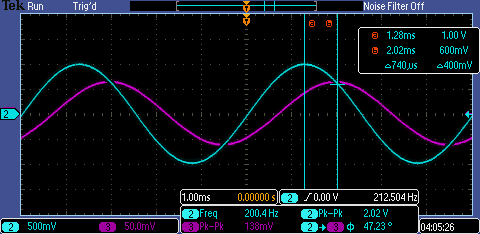
Experimental measurements:
Magnitude of Vout (left image) and phase delay between Vout and Vin (right image) are shown on the following oscilloscope screenshots:
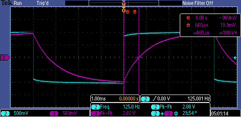
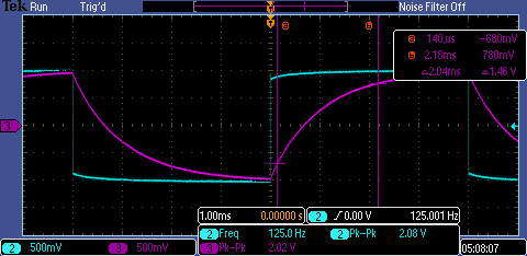
Part 3 - Analysis of Fig. 1.24
Circuit and hand calculations:
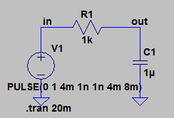
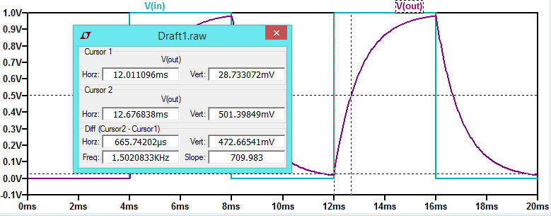
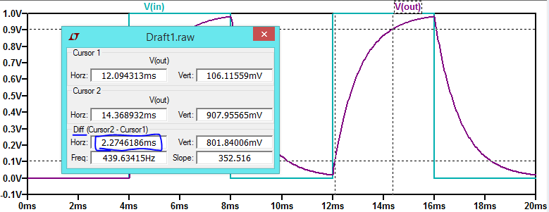
Simulations in LTSpice:
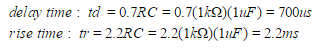
Delay time is the time it takes the output to reach 50% of the input voltage
Rise time is the time it takes for the output to go from 10% to 90% of the input:
Experimental measurements:
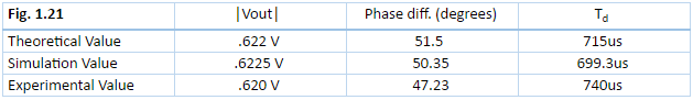
Finally, one more table to summarize how well the theoretical, simulation, and experimental values correlate:
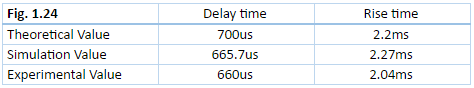
The values calculated closely match those found with both simulation and experimental measurement.
All work done in this lab is backed up: