
Lab 8 - EE 420L
Lab Work
Note: For the following lab, CD4007UBE was used instead of the CD4007CN.
NMOS Characterization
The following simulations are done in XY mode with a persistance of infinity. Depending on the type of simulations, whichever source is varying will be the function generator and the other source(s) are supplied through the DC power supply. The function generator must be in ramp mode, where the amplitude is the highest value, where the offset is half of the amplitude. When probing, the x-axis is the function generator and the y-axis is the drain of the MOSFETs.
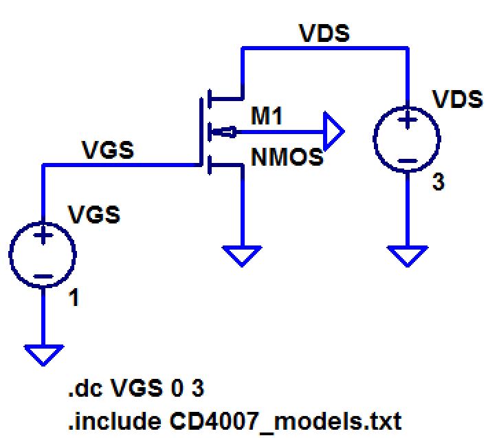
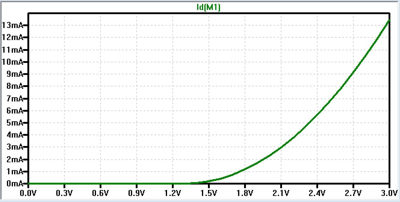
ID vs. VGS (0 < VGS < 3V) with VDS = 3V
| Schematic | |
| Actual Simulation | |
| LTspice Simulation | |
ID v. VDS (0 < VDS < 5 V) for VGS varying from 1 to 5 V in 1V steps
| Schematic |  |
| VGS = 1V |  |
| VGS = 2V | 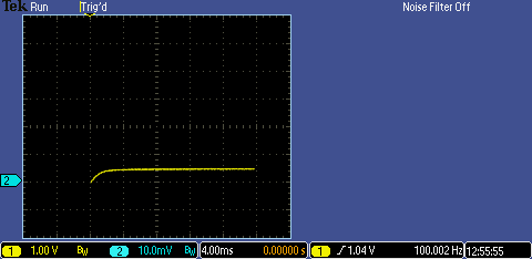 |
| VGS = 3V | 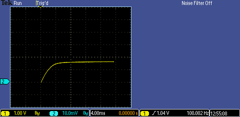 |
| VGS = 4V | 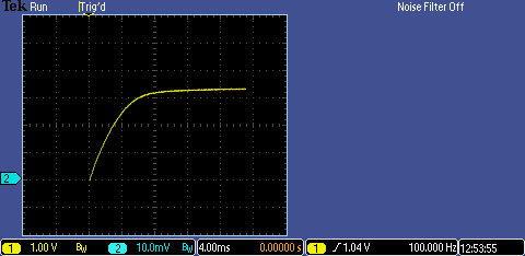 |
| VGS = 5V |  |
| LTspice Simulation | 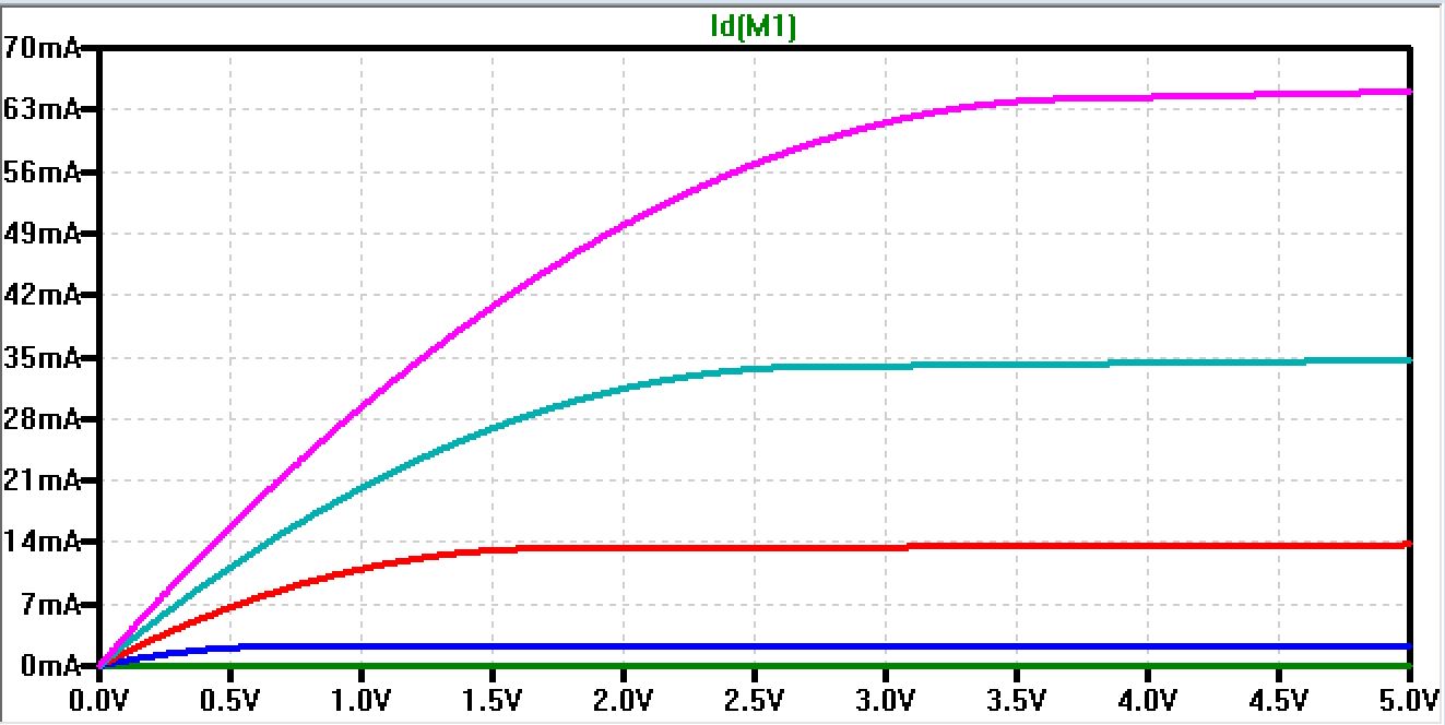 |
ID v. VGS (0 < VGS < 5V) with VDS = 5V for VSB varying from 0 to 3 V in 1 V steps
For this experiment, when VSB goes up 1 volt, the offset of VGS and VDS must go up 1 volt to keep VDS at 5 volts.
| Schematic | 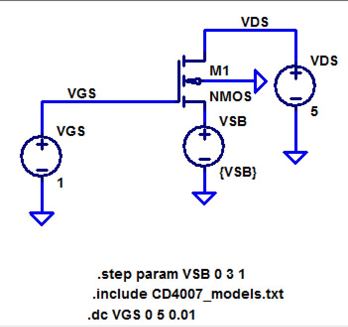 |
| VSB = 0V VDS = 5V | 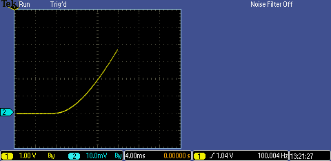 |
| VSB = 1V VDS = 6V | 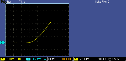 |
| VSB = 2V VDS = 7V | 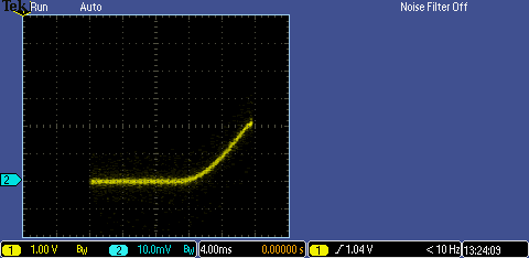 |
| VSB = 3V VDS = 8V | 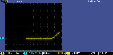 |
| LTspice Simulation | 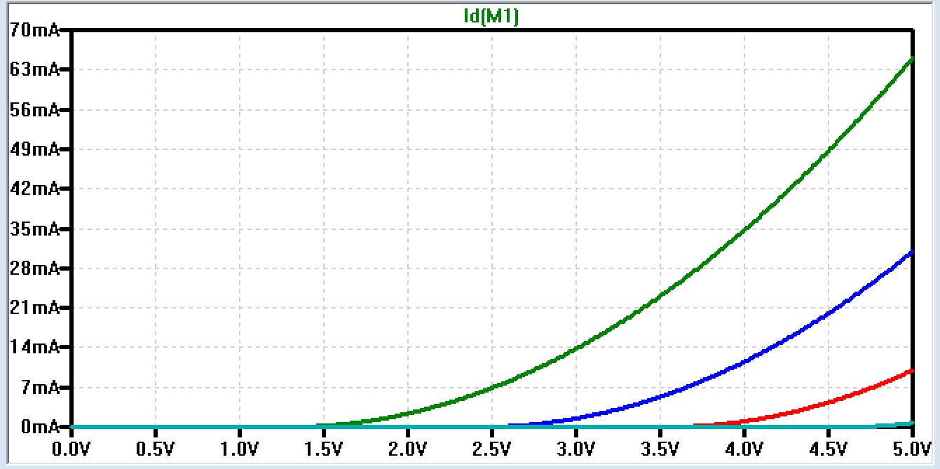 |
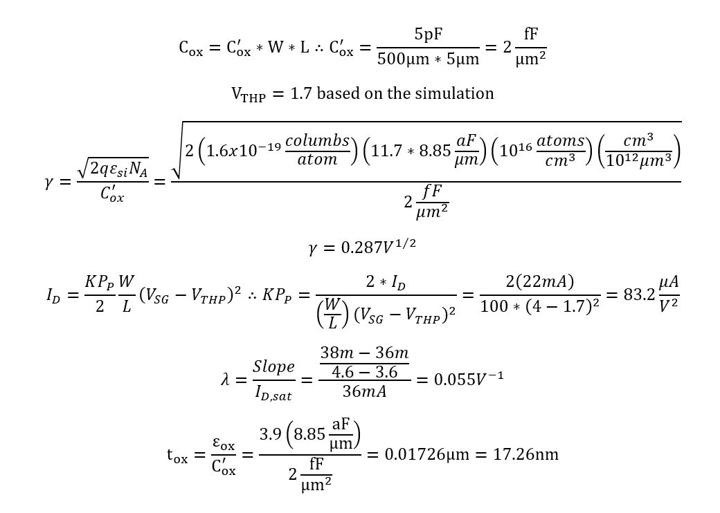
Calculations for NMOS MODEL

The NMOS parameters that were found and used in the LTspice simulations were close to the actual simulations. The simulations could match up better by fixing a few of the parameters in the text file.
PMOS Characterization
The same procedures done for the NMOS must be done for the PMOS.
ID vs. VSG (0 < VSG < 3V) with VSD = 3V
| Schematic |  |
| Actual Simulation |  |
| LTspice Simulation | 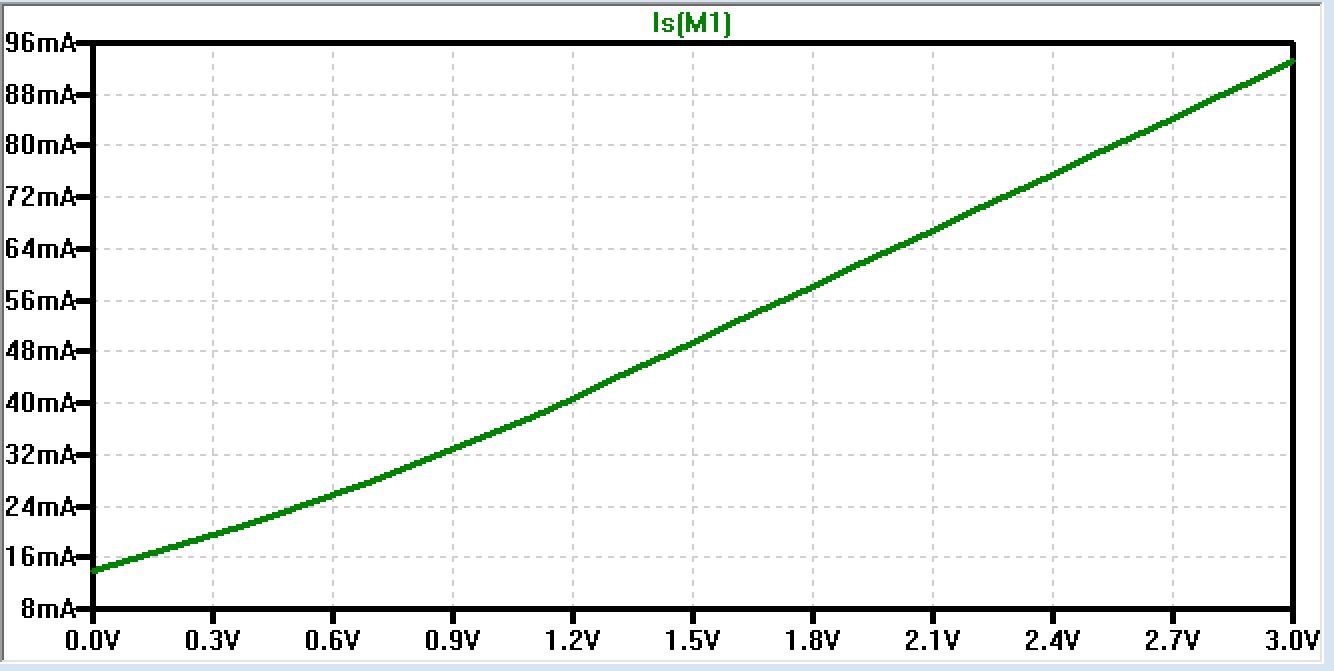 |
ID v. VSD (0 < VSD < 5 V) for VSG varying from 1 to 5 V in 1V steps
| Schematic | 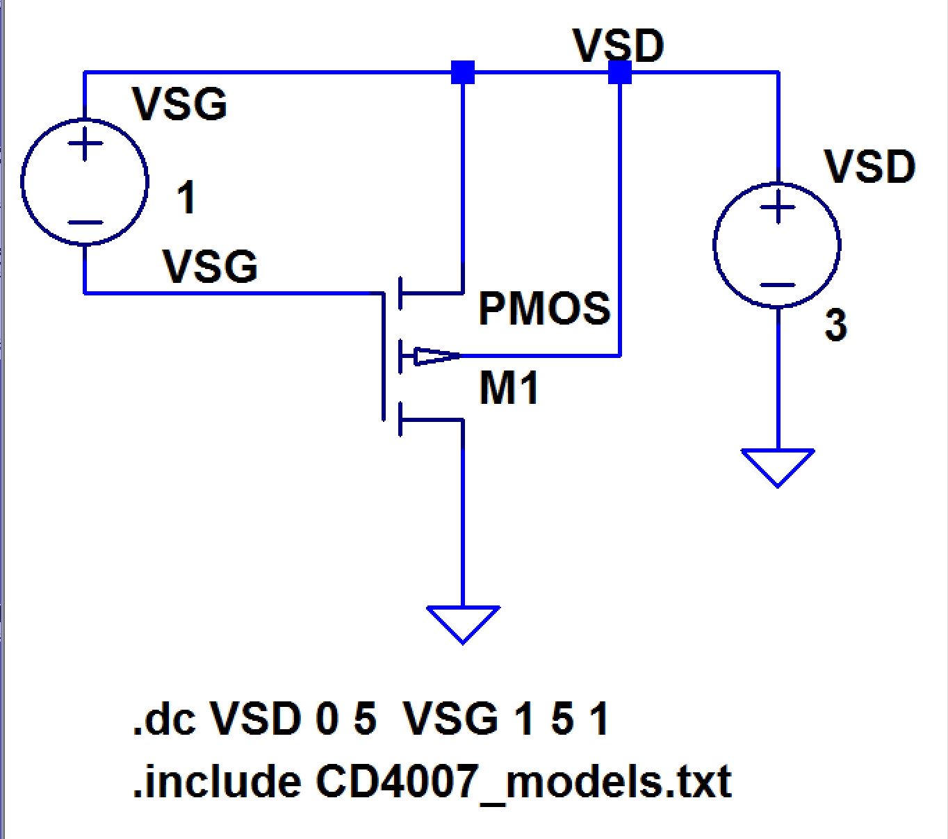 |
| VSG = 1V | 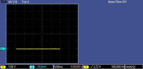 |
| VSG = 2V | |
| VSG = 3V | 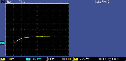 |
| VSG = 4V |  |
| VSG = 5V | 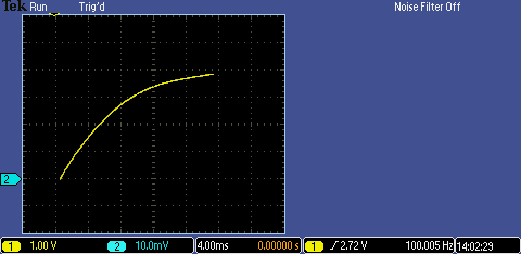 |
| LTspice Simulation | 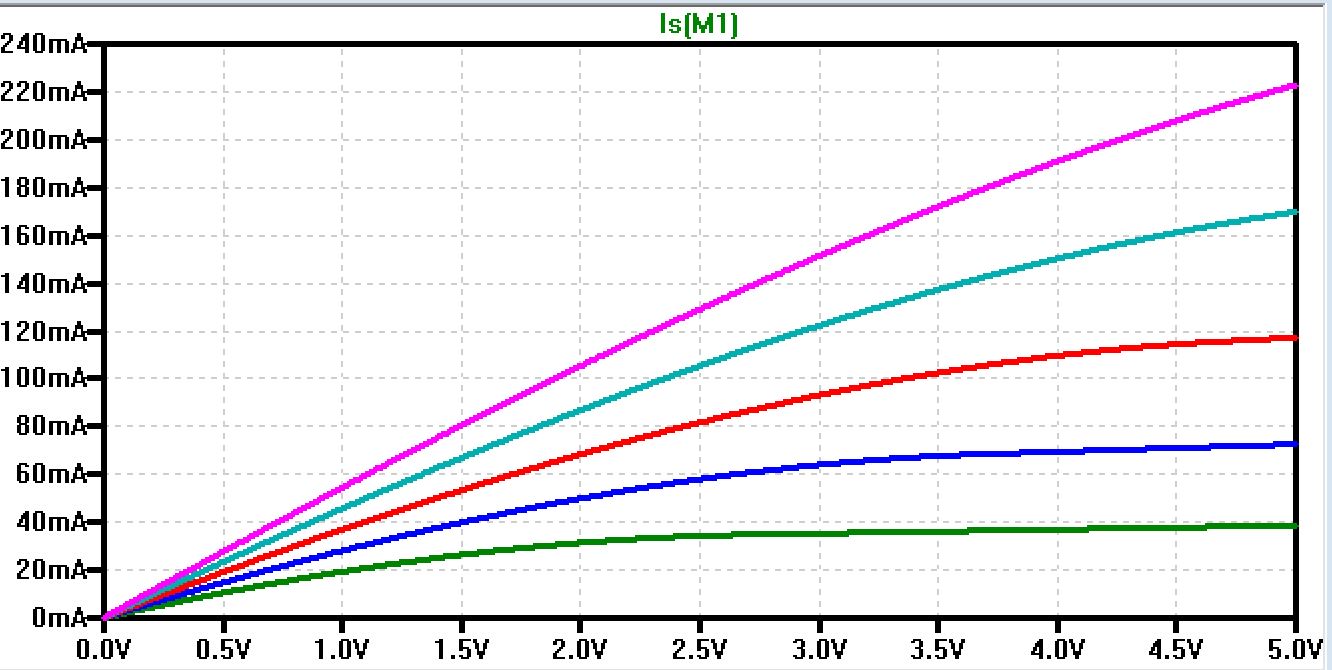 |
ID v. VSG (0 < VSG < 5V) with VSD = 5V for VBS varying from 0 to 3 V in 1 V steps
The VBS starts at 5 volts, so the actual VBS value is 0 volt since the source value is being subtracted by 5 volts.
| Schematic | 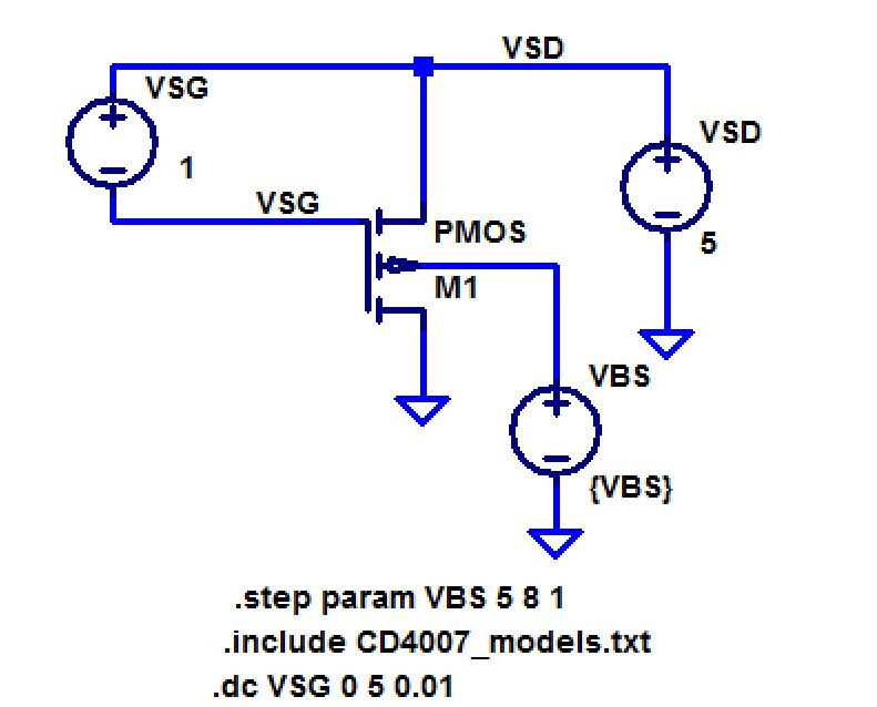 |
| VSB = 0V | |
| VSB = 1V | 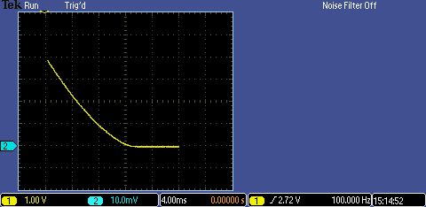 |
| VSB = 2V |  |
| VSB = 3V | 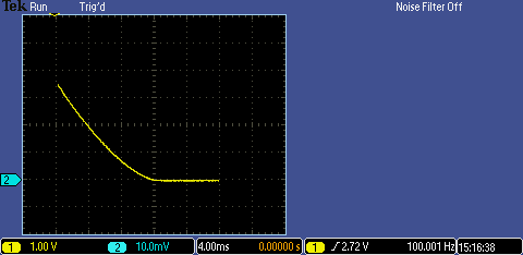 |
| LTspice Simulation |  |
Calculations for PMOS MODEL
Overall, the parameters that I calculated and simulated in LTspice for the PMOS did not closely match the actual simulation; therefore, changes are needed to made. The reasoning for the simulations not closely matching up may be due to the actual schematics that were created for both experiments.

Measuring Delay of an Inverter
Below is the schematic of the inverter to measure of the delay to determine if the MOSFET devices are accurate. A 15pF load is attached to the output due to capacitance of the probe and other capacitors that are factored in the inverter.
| Schematic |  |
| Actual Simulation | 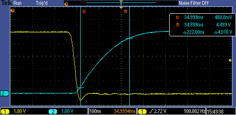 |
| LTspice Simulation |  |
Based on the two simulations, the delay in the actual simulation is double of the value of the delay in the LTspice simulations. The reasoning behind it is because the PMOS model is not accurate to the simulations. I need to redo the simulation of the ID v. VSG to have a better result to model the PMOS device.