Lab 7 - EE 420L 

Authored by Sharyn Miyaji,

Email: miyajis@unlv.nevada.edu

Today's date: Wednesday, March 29, 2017


Pre-Lab Work


Lab Work


Design an audio amplifier (frequency range from roughly 100 Hz to 20 kHz) assuming that you can use as many resistors, ZVN3306A transistors, and ZVP3306A transistors as you need along with only one 10 uF capacitor and one 100 uF capacitor. Assume that the supply voltage is 10 V, the input is an audio signal from an MP3 player (and so your amplifier should have at least a few kiloohms input resistance), and the output of your design is connected to an 8-ohm speaker (so, ideally, the output resistance of your amplifier is less than 1 ohm).


Designing an Audio Amplifier


First, we were given a zip file (lab7_sims.zip) to compare the simulation with and without the speakers to see the difference in results.  As seen in the simulation below, the schematic without the amplifier basically outputs a flat line because the AC voltage is close to zero since the voltage divider value is close to zero; therefore, there is a huge votlage drop across the 10k resistor and nothing will come out of the speaker.  With the amplifier, the gain from the push-pull amplifier is about 300 V/V using the transconductance value calculated from lab 6 and 100k resistor connected between the drain and gate of the transistors.  Although there is an output with the push-pull amplifier, the gain is not high enough due to the output resistance value of the amplifier.


SchematicSimulation
http://cmosedu.com/jbaker/courses/ee420L/s17/students/miyajis/lab7/Lab7_audiobefore_schematic.JPGhttp://cmosedu.com/jbaker/courses/ee420L/s17/students/miyajis/lab7/Lab7_audiobefore_sim.JPG
   

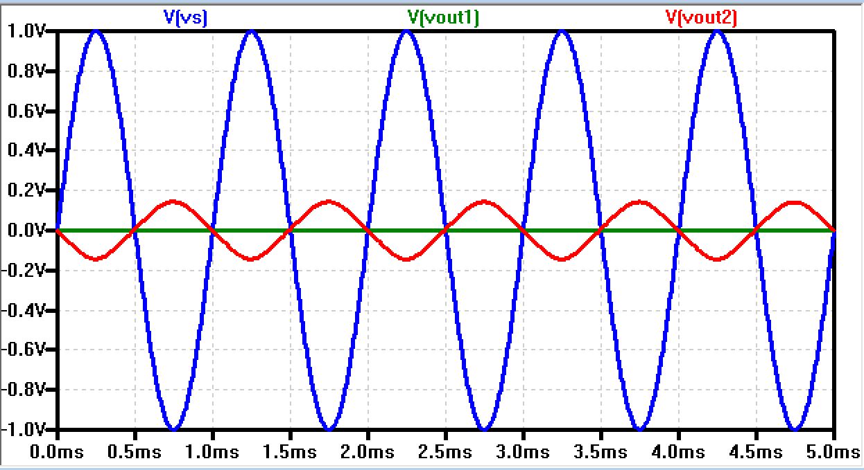
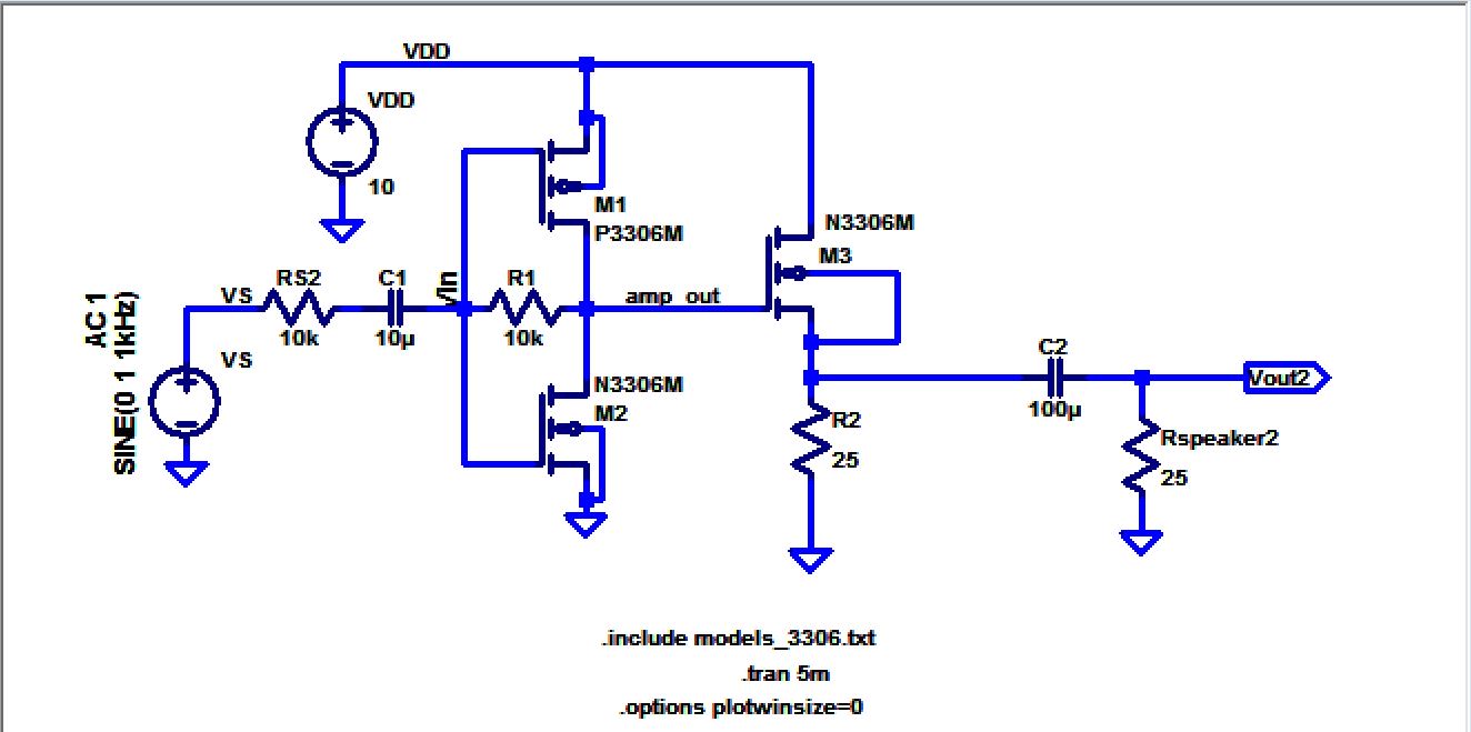
In order to decrease the output resistance of the push-pull amplifier and increase the gain of the circuit, an NMOS source follower amplifier can be added after thepush-pull amplifier to increase the output value.  The reasoning for choosing an NMOS source follower rather than a PMOS source follower is so that the circuit does not draw more current than it already will be since the DC power supply must be increase to 10V instead of 5V.  Note: the speakers given is 25 ohms rather than 8 ohms.  Below is the modified circuit with the two different resistance value of R2.


Schematic Simulation
http://cmosedu.com/jbaker/courses/ee420L/s17/students/miyajis/lab7/Lab7_audioafter_schematic.JPGhttp://cmosedu.com/jbaker/courses/ee420L/s17/students/miyajis/lab7/Lab7_audioafter_sim.JPG
http://cmosedu.com/jbaker/courses/ee420L/s17/students/miyajis/lab7/Lab7_audioafter_schematic2.JPGhttp://cmosedu.com/jbaker/courses/ee420L/s17/students/miyajis/lab7/Lab7_audioafter_sim2.JPG


Although we would like to get the output resistance as close to 1 ohms as possible, the output of the 2-stage amplifier works better theoreotically with a 25 ohm resistor attached to the source of the NMOS rather than a 8 ohm resistor because it is close to the resistance of the speaker.  Below is the input and output resistance of the audio amplifier, where R2 is 25 ohms.


Input Resistance of 10khttp://cmosedu.com/jbaker/courses/ee420L/s17/students/miyajis/lab7/Lab7_InputResistance.JPG
Output Resistance of 12.5http://cmosedu.com/jbaker/courses/ee420L/s17/students/miyajis/lab7/Lab7_OutputResistance.JPG


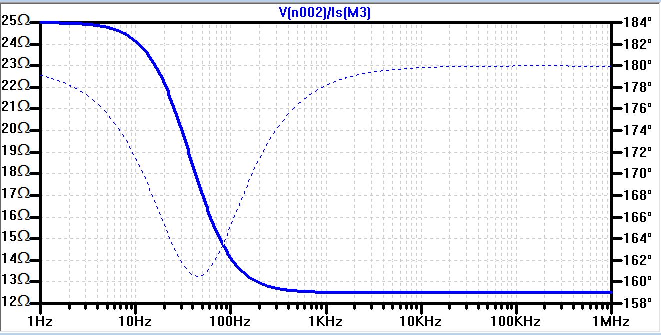
Experimental Results   


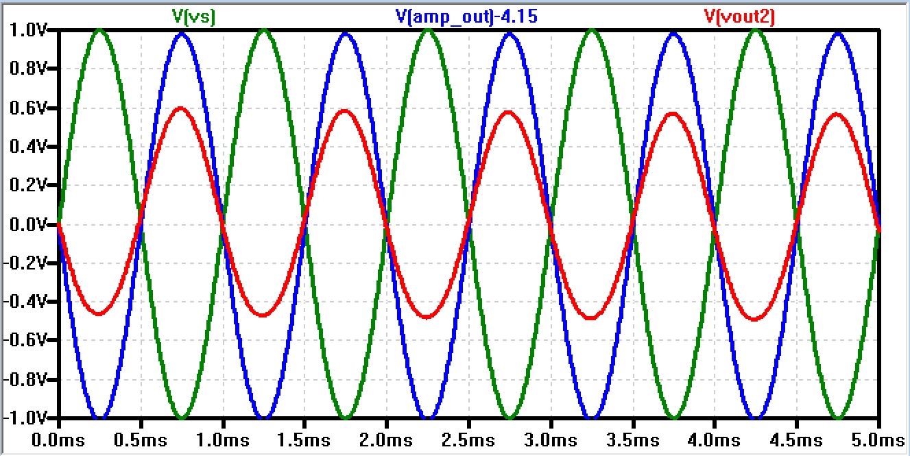
Below are the experimental results of the audio amplifier with and without the speakers, where the yellow signal is the input and the blue signal is the output.  Also the output of the push-pull amplifier was checked to make sure that actual and theoretical values are almost the same.  The actual simulations are not too far off of the theoretical simulations in LTspice.


Amplifier Simulationhttp://cmosedu.com/jbaker/courses/ee420L/s17/students/miyajis/lab7/Amplifier_Output.PNG
Circuit Simulation without Speakershttp://cmosedu.com/jbaker/courses/ee420L/s17/students/miyajis/lab7/Circuit_Output.PNG
Circuit Simulation with Speakers
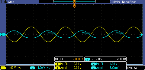
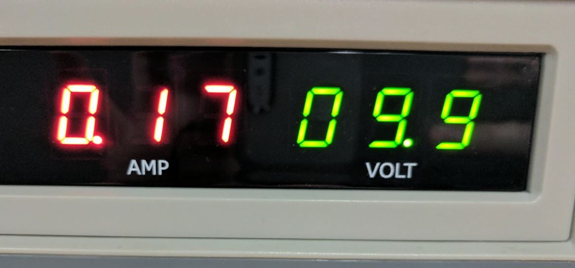
http://cmosedu.com/jbaker/courses/ee420L/s17/students/miyajis/lab7/Output_Speakers.PNG
   

Power Dissipation

   
DC Power Supply

http://cmosedu.com/jbaker/courses/ee420L/s17/students/miyajis/lab7/Lab7_PowerDissipation.JPG

To calculate the power dissipation in the circuit, the voltage and current are measured in the DC power supply.  Based on the values measued, the two values are multiplied since P = V*I, which equal 1.683W.  This audio amplifier design caused the transistors to heat up due to the amount of current flowing throughout the circuit.  


Return to Sharyn's EE420L Labs 

Return to EE 420L Labs