

Lab 6 - EE 420L
Lab Work
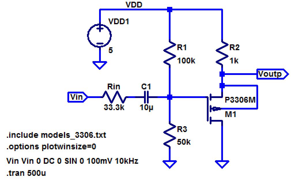
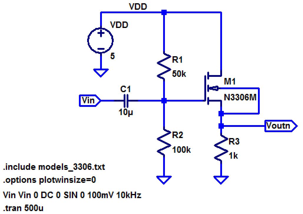
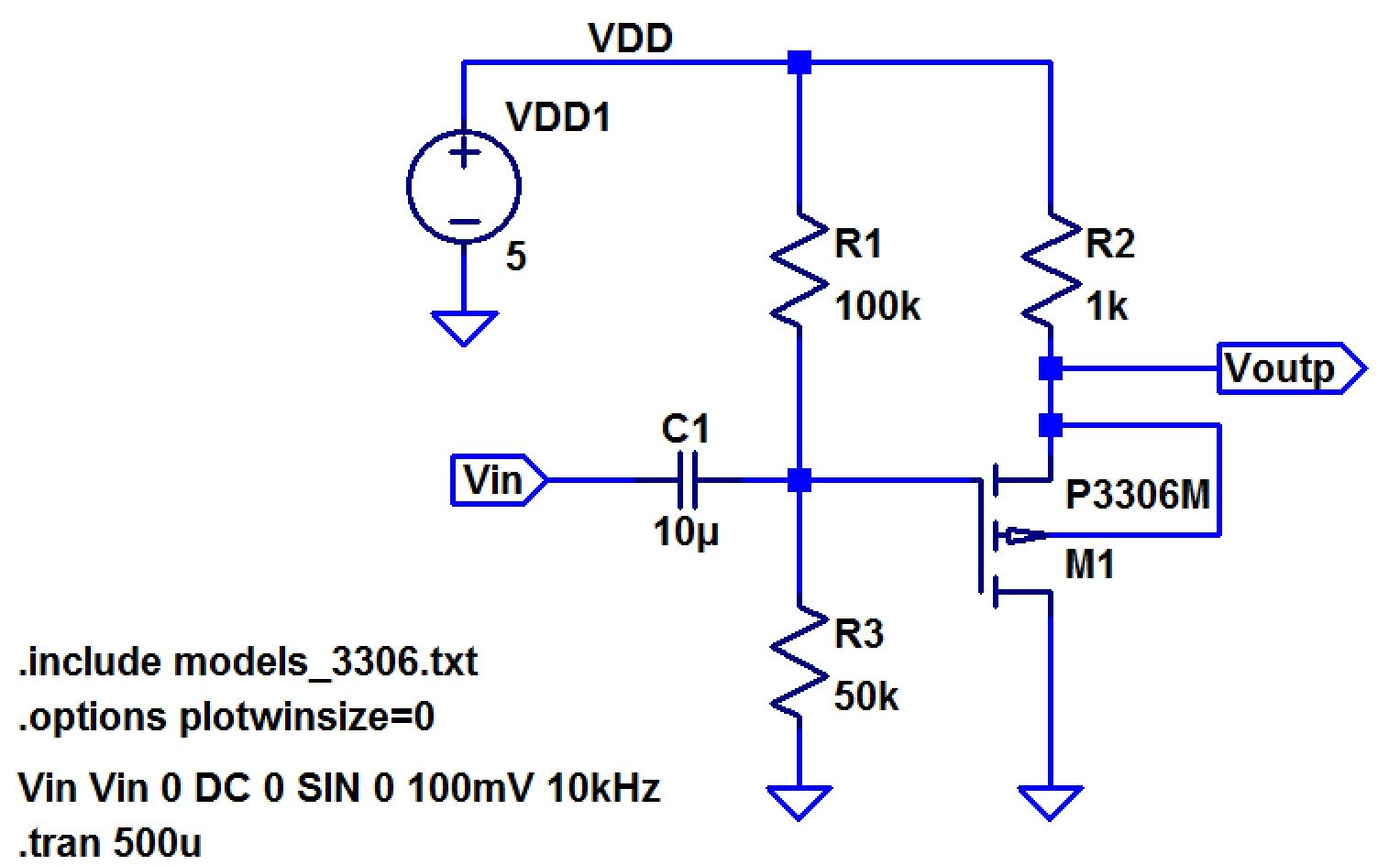
Source Followers Amplifiers (a.k.a. Common-Drain Amplifiers)
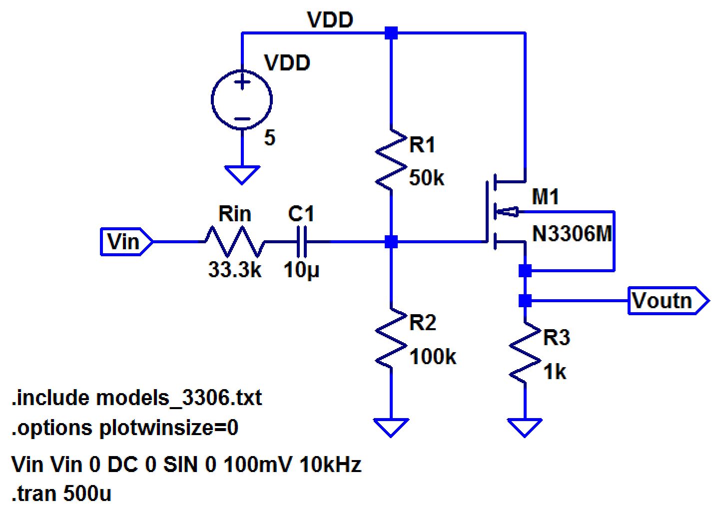
Below are schematics for NMOS and PMOS source followers amplifiers (also known as common-drain amplifiers).
In your lab report discuss the operation of these circuits.
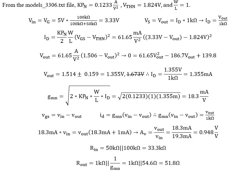
In a common drain amplifier, the drain of the amplifier is common for both the input and the output. The input is at the gate of the gate of the transistor and the output is measured at the source. The input resistance for both cases can be found by calculating the resistors connected to the gate in parallel. The output resistance can be found by calculating the resistor connected to the source of the transistor in parallel with 1/gm since they are connected to the output. In order to find the transconductance of the transistor, the DC voltages and drain current must be found. To find the DC voltage at the gate or the input voltage, voltage division must be applied with VDD and to find the DC voltage at the source, KCL and the square law equation are applied, which determines the DC output voltage. Once those DC voltages are found, the drain current throughout the circuit, which can also determine the transconductance of the transistor, can be determined.
Simulate the operation of these amplifiers.
| NMOS | PMOS |
| |
| |
| NMOS | PMOS | |
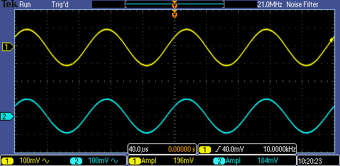
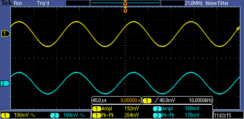
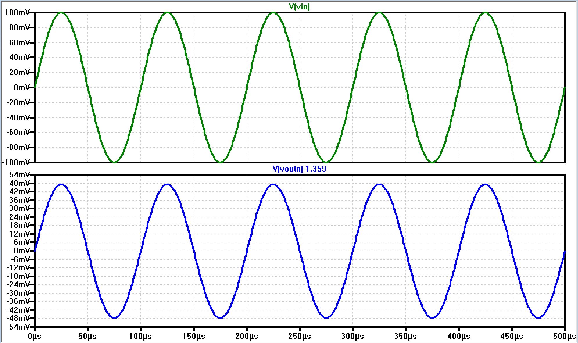
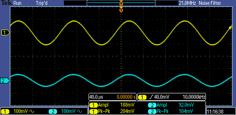
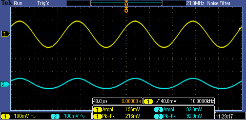
| Calculated Gain | 0.948V/V | 0.918V/V |
| Experimental Gain | 0.939V/V | 0.863V/V |
| Input Resistance | 33.3k | 33.3k |
| Output Resistance | 48 | 77 |
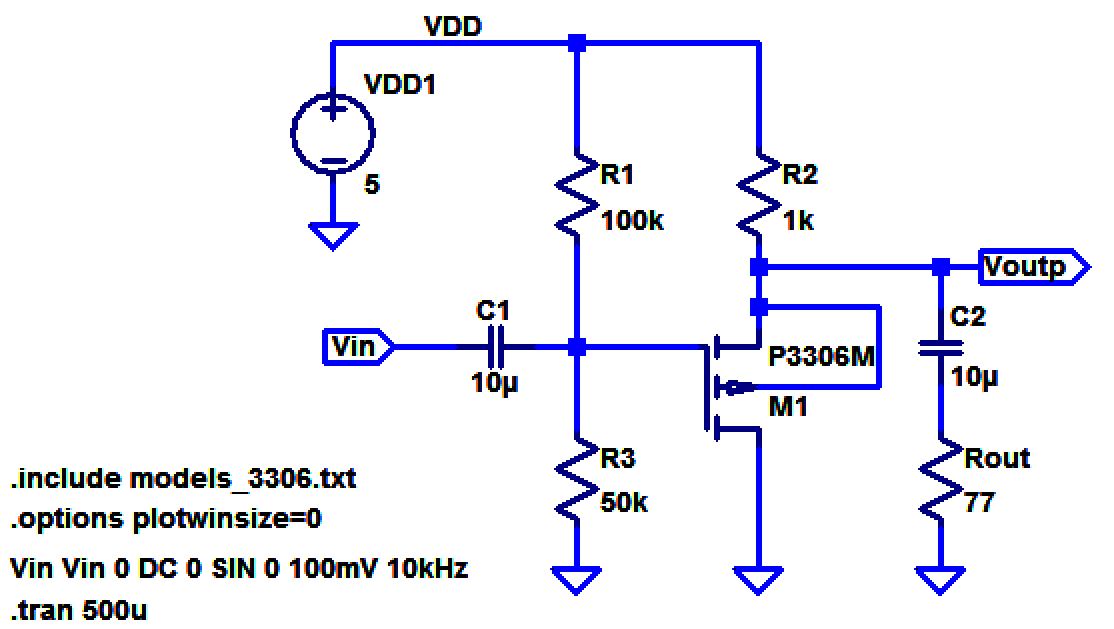
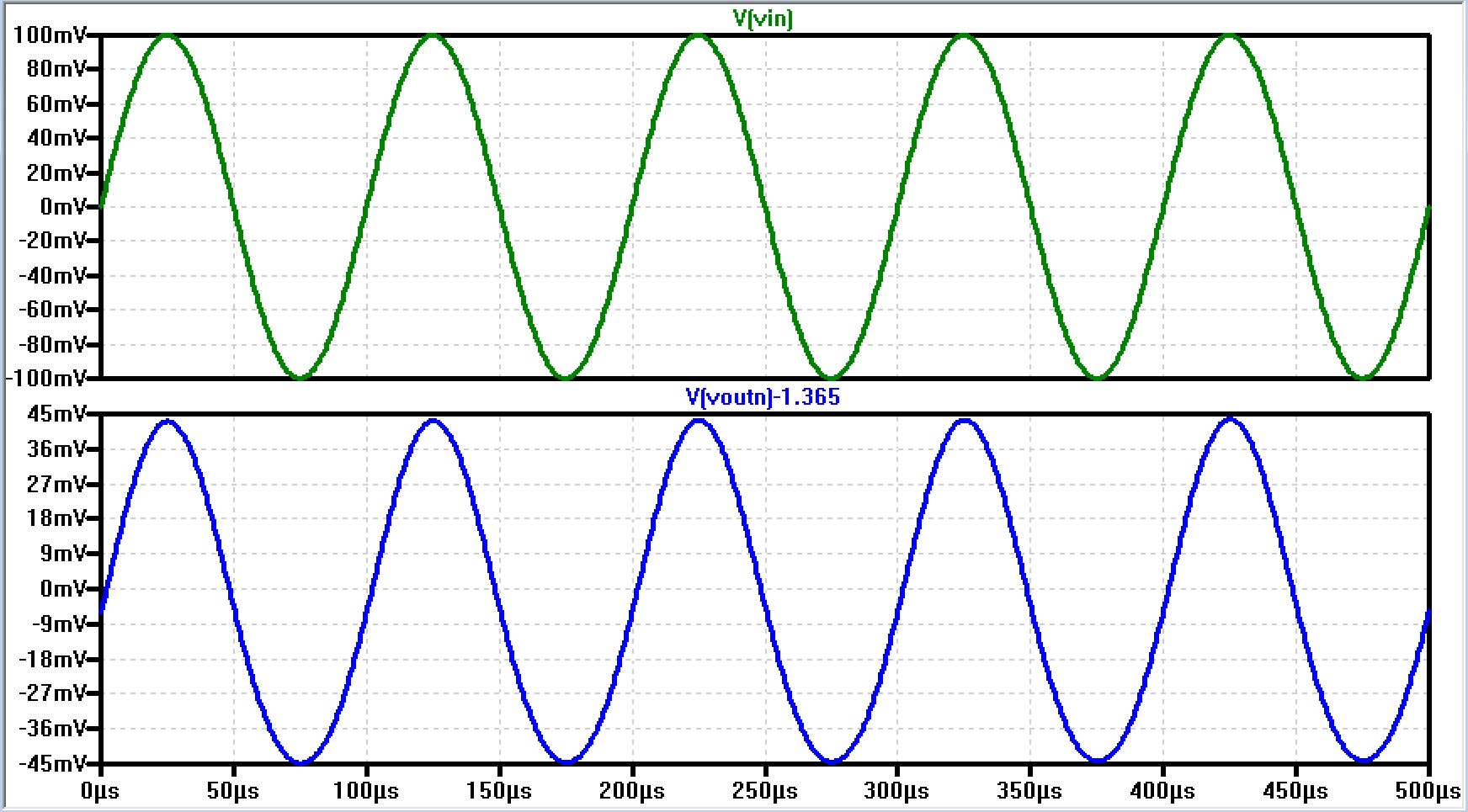
Common-Source Amplifiers
Below are two common-source amplifiers.
| NMOS | PMOS |
 | 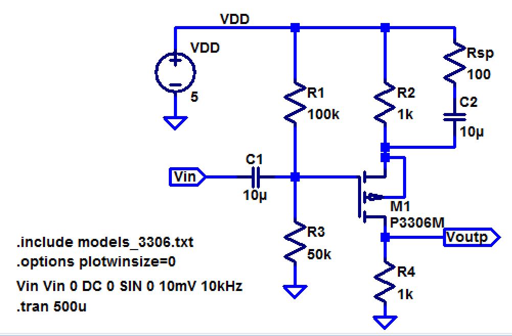 |
Discuss the operation of these amplifiers in your lab report including both DC and AC operation.
Using voltage division and KCL, the DC and AC voltages and current can be found. The DC gate voltage is the same as the CD amplifier since the value of the resistors and VDD the same. The DC output voltage is a different value since it is measured between the drain of the transistor and a 1k resistor that is tied to VDD for the NMOS and ground for the PMOS. The source resistance for both circuits causes the gain of the circuit to be higher that the CD amplifier since the resistance in the drain is lower and the capacitor connected in series is for AC coupling.
Hand calculate the gains and the input/output resistances.
| NMOS | PMOS |
 |  |
Again compare your hand calculations to simulation and experimental results.
| NMOS | PMOS | |
| Gain Schematic (Same as above) | | |
| Theoretical Gain Simulation | 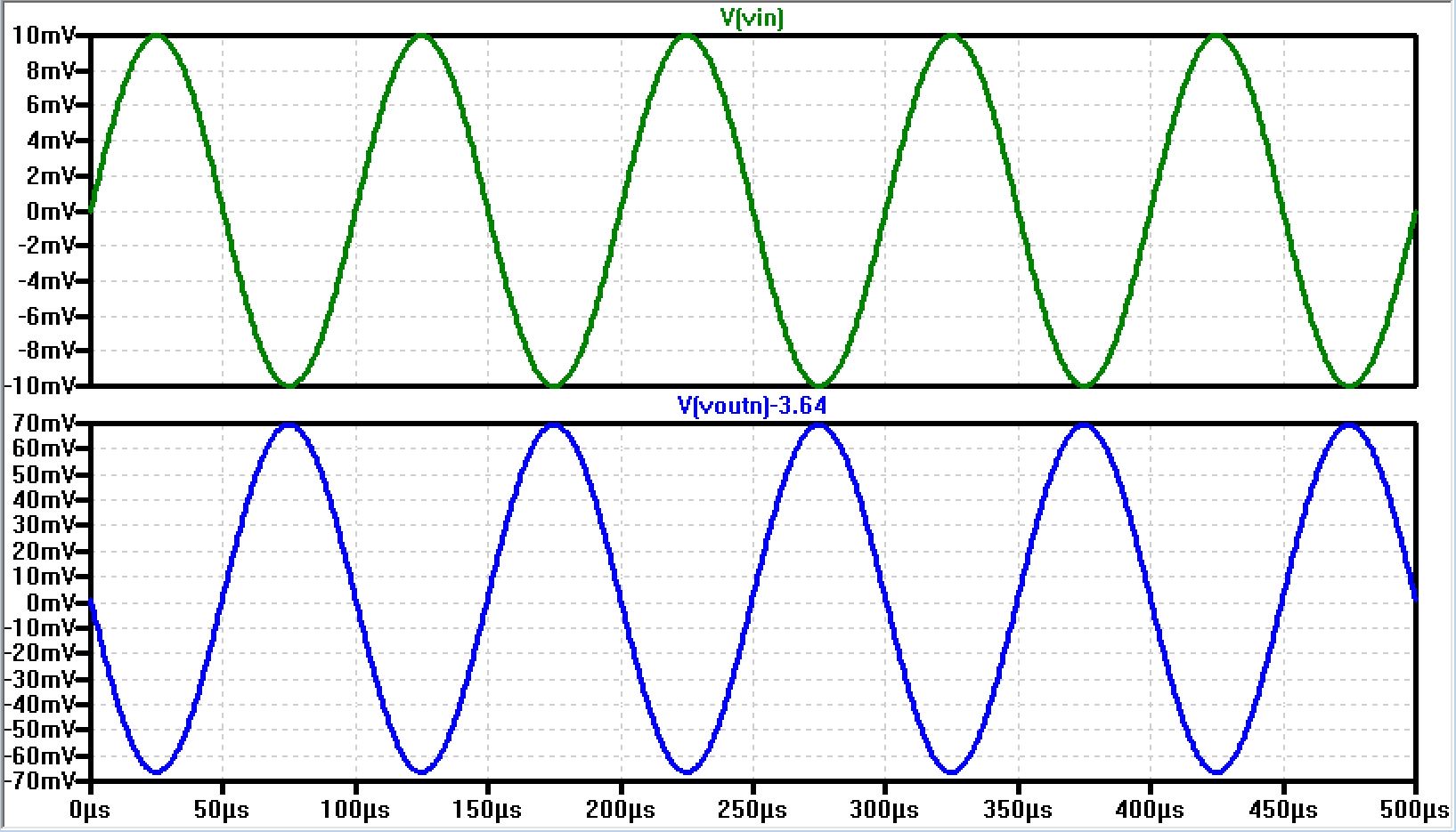 | 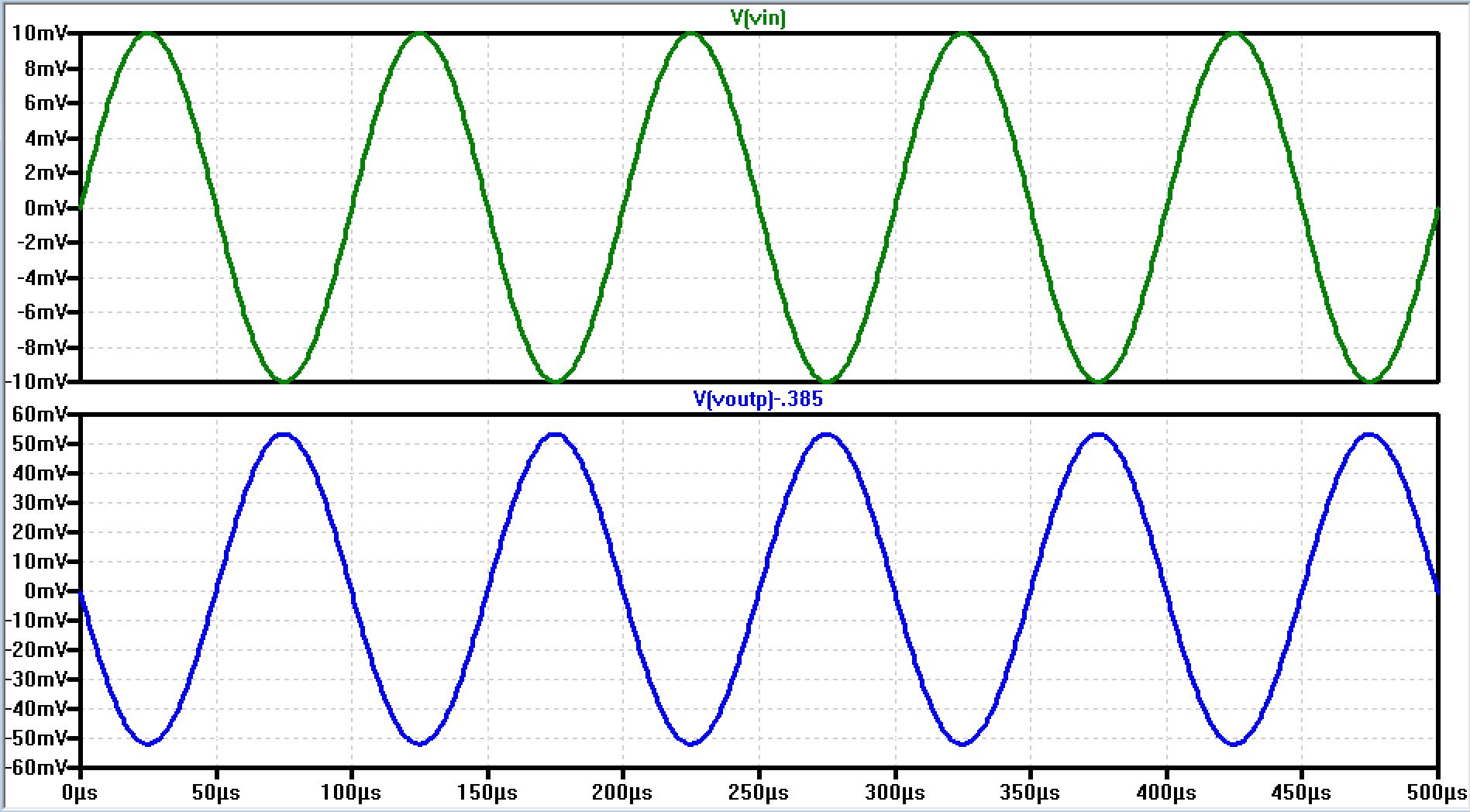 |
| Experimental Gain Simulation | 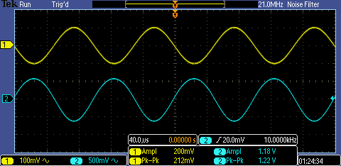 |  |
| Input Resistance Schematic | 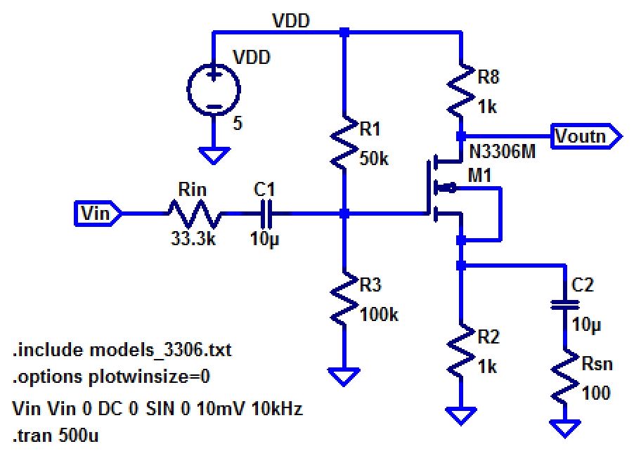 |  |
| Theoretical Input Resistance Simulation |  | 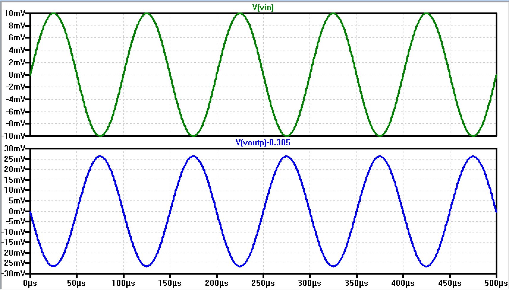 |
| Experimental Input Resistance Simulation |  | 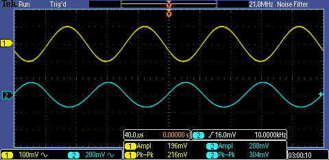 |
| Output Resistance Schematic |  |  |
| Theoretical Output Resistance Simulation | 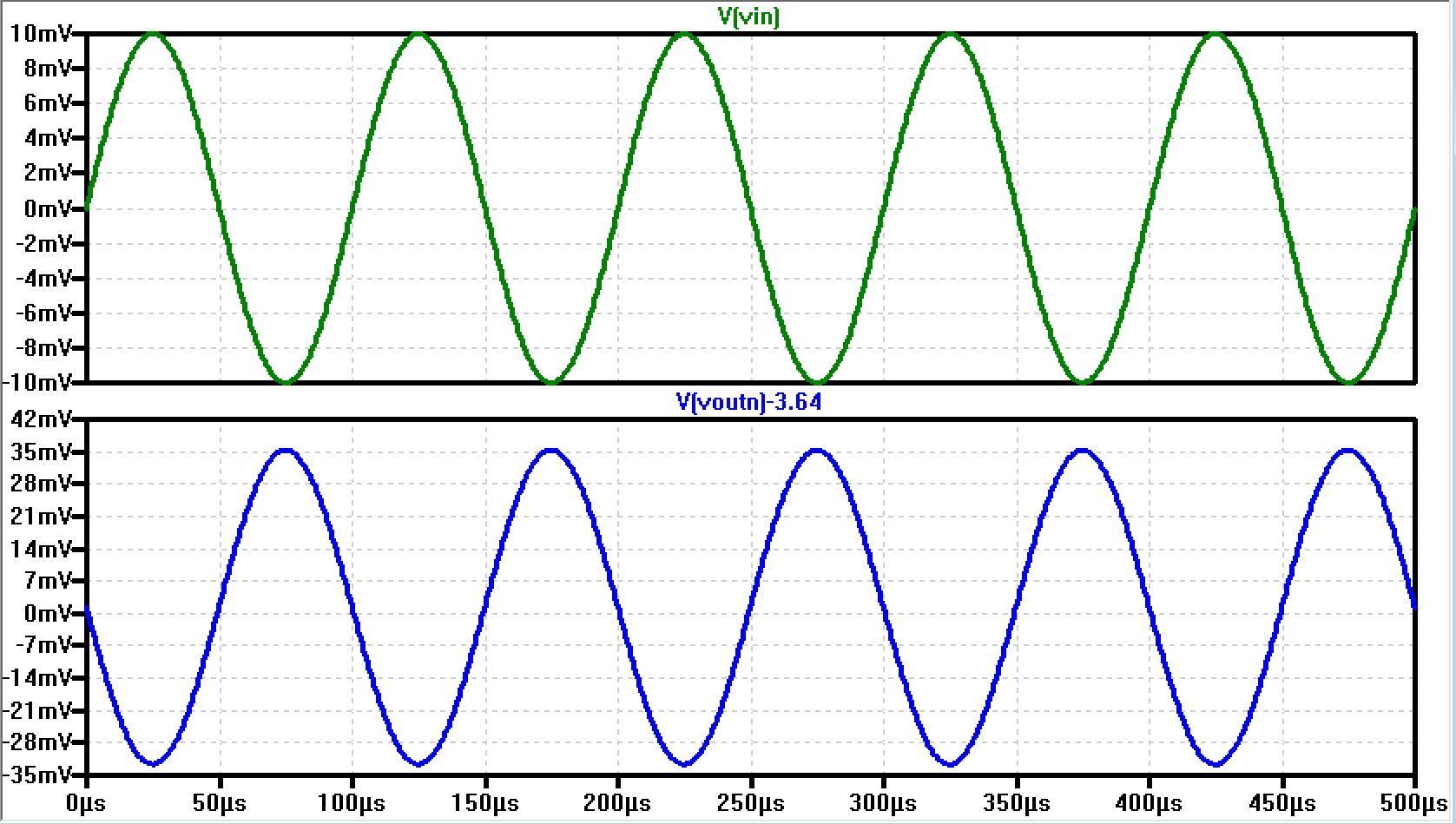 |  |
| Experimental Output Resistance Simulation | 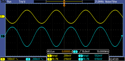 |  |
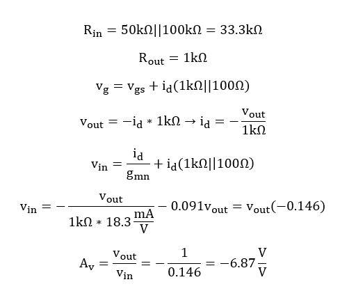
| NMOS | PMOS | |
| Calculated Gain | -6.87V/V | -5.55V/V |
| Experimental Gain | -5.75V/V | -2.78V/V |
| Input Resistance | 33.3k | 33.3k |
| Output Resistance | 1k | 1k |
| NMOS | PMOS |
 |  |
| NMOS | PMOS |
 |  |
| NMOS | PMOS | |
| Gain Schematic (Same as above) | | |
| Theoretical Gain Simulation | 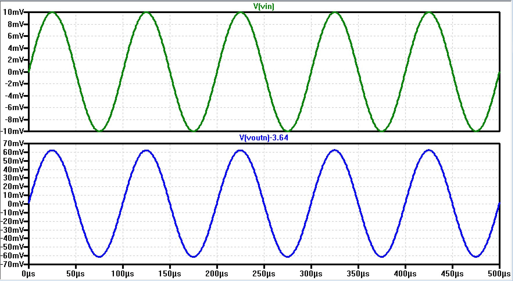 | 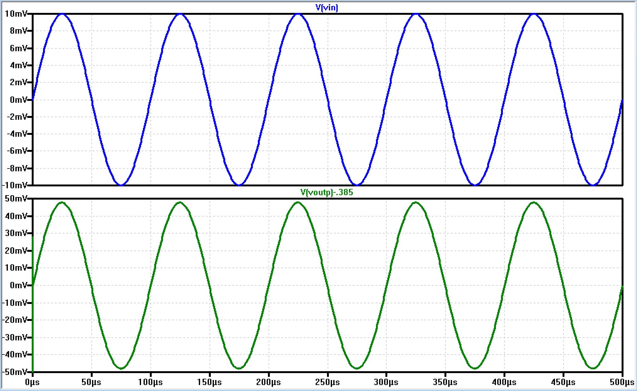 |
| Experimental Gain Simulation | 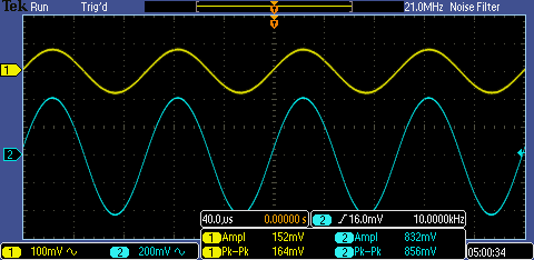 |  |
| Input Resistance Schematic | 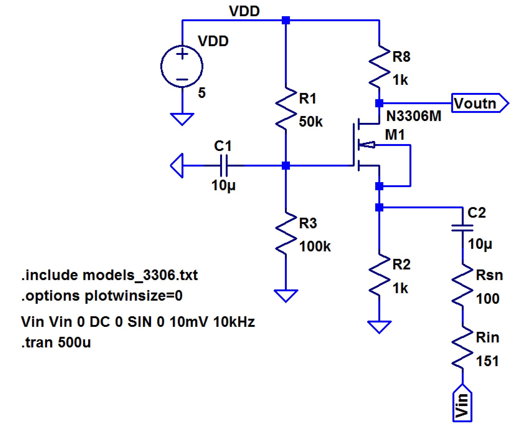 | 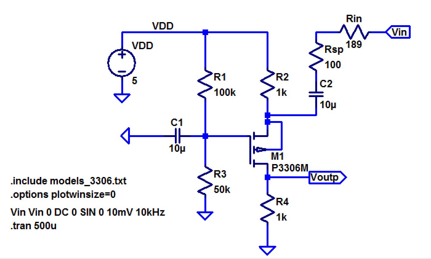 |
| Theoretical Input Resistance Simulation |  |  |
| Experimental Input Resistance Simulation | 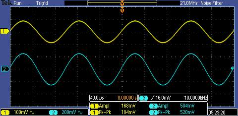 | 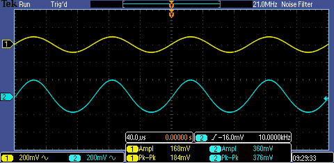 |
| Output Resistance Schematic |  | 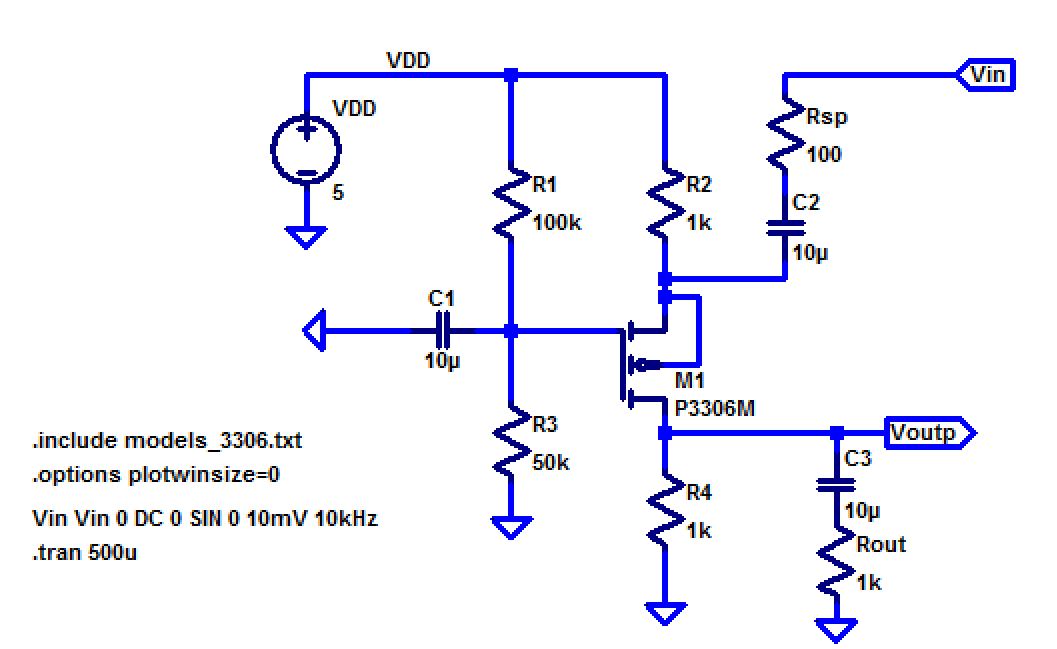 |
| Theoretical Output Resistance Simulation | 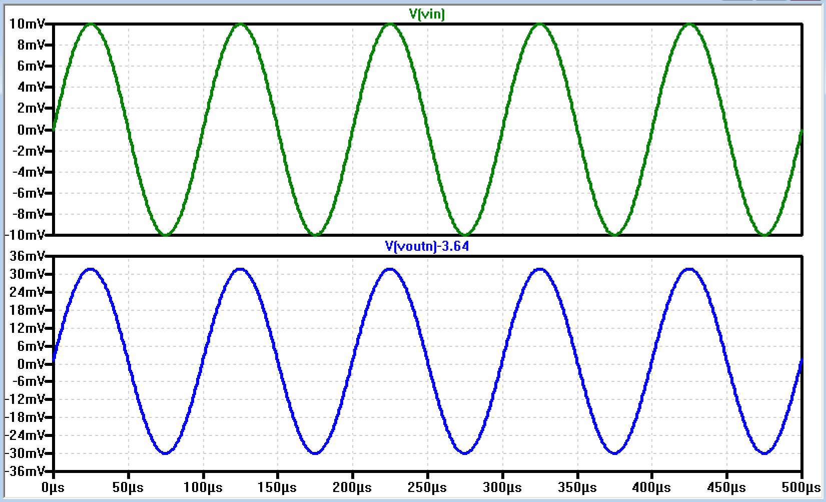 |  |
| Experimental Output Resistance Simulation | 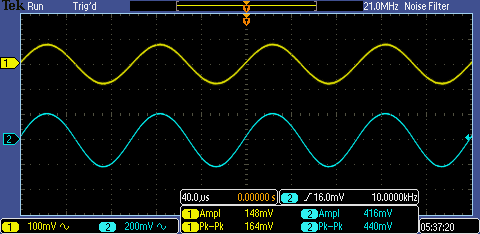 |  |
Results
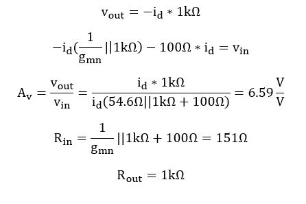
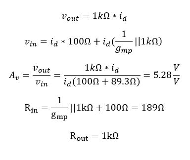
| NMOS | PMOS | |
| Calculated Gain | 6.59V/V | 5.28V/V |
| Experimental Gain | 5.22V/V | 3.27V/V |
| Input Resistance | 151 | 189 |
| Output Resistance | 1k | 1k |
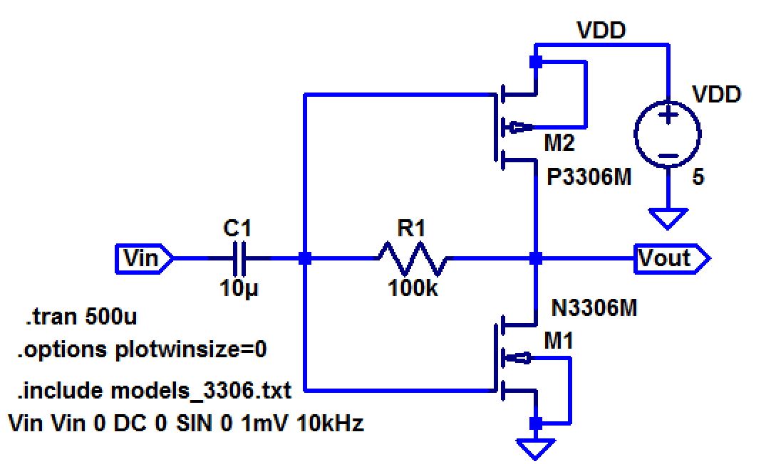
Push-Pull Amplifier
Below is a push-pull amplifier.
Discuss the operation of this amplifier in your lab report including both DC and AC operation.
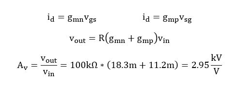
The push-pull amplifier will depend on the DC voltage offset since it will determine if the NMOS or PMOS is on and off. They both cannot be on the same time, so if the DC voltage is low, the NMOS is off and if the DC voltage is high, the PMOS is off. To find the gain, the transconductance of both the NMOS and PMOS must be added together and multiplied by the resistor between the gates and drains of the transistor based on nodal analysis.
Hand calculate the gain of this amplifier.
Since the push-pull amplifier contains both an NMOS and PMOS, it can be good at sourcing or sinking current because the NMOS sinks the current since it is tied to ground and the PMOS sources the current since it is tied to VDD.
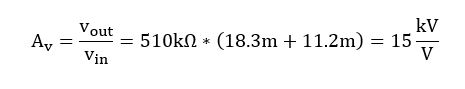
If the 100k resistor were to be replaced with the 510k resistor, the gain of amplifier will increase and have a higher chance of making the output voltage to clip since it will swing out of its range. Therefore, the input voltage needs to be really small in order to create a nice waveform.
Again compare your hand calculations to simulation and experimental results.
| 100k Resistor | 510k Resistor |
|  |
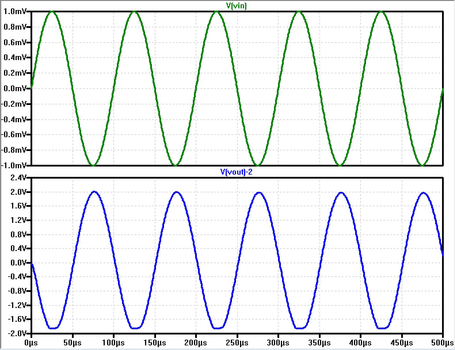 |  |
 | 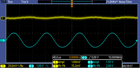 |
| Gain = 1.48V/2mV = 740 V/V | Gain = 2V/2mV = 1kV/V |
The amplifier with the 510k resistor looks a little saturated compared to the amplifier with the 100k resistor. The values for both gains were far off the ones that were calculated, especially the amplifier with the 510k resistor.
Most of the experimental values were not the same as the theoretical values, which may be because the body voltages were not taken into consideration. Normally, the body of the NMOS is tied to ground and the PMOS is tied to VDD. Also the PMOS were constantly changed because it was not giving a close output since it may have not been good.