Lab 3 - EE 420L
This lab will utilize the LM324 op-amp (LM324.pdf).
Review the data sheet for this op-amp.
For the following questions and experiments assume VCC+ = +5V and VCC- = 0V.Questions

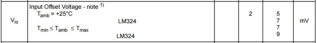
A good estimate for the offset voltage is 2mV because it is the typical value on the datasheet. The maximum offset voltage possible is 9mV in worst case scenarios.
For this experiment, the following schematic is built and tested.
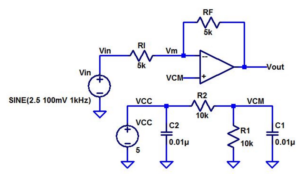
What is the common-mode voltage VCM? Does VCM change? Why or why not?
The common mode voltage is 2.5V because the voltage divider (2 10k resistors in parallel) causes the input DC voltage to cut in half. The VCM does not change because the DC power supply and 2 10k resistors are constant value and AC voltage source does not affect VCM in this case.
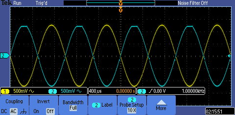
Since the circuit using an inverting amplifier, the closed loop gain is equal to -RF/RI = -(5k)/(5k) = -1, which causes the simulation to be 180 degrees out of phase of the input voltage.
What is the output swing and what is it centered around?
-What happens if the input isn't centered around around VCM, that is, 2.5 V?
-Provide a detailed discussion illustrating that you understand what is going on.
Since the AC voltage source is supplying a DC offset of 2.5V with a 100mV amplitude/swing, the output swings 2.5 ± 0.1 V, which is between 2.4 to 2.6 V. Based on the simulation, the swing is 250mV, so the output swings between 2.25 and 2.75 V. It is centered around 2.5 V due to the DC offset of 2.5V. If the input is not centered around around VCM, it can cause the output to clip because the output cannot go out of the 0 to 5 volt range. As the VCM increases, the Vout simulation will increase and eventually reach 5 volts or even more in a theoretical calculation, which would actually result in clipping since the output cannot exceed 5 volts.
What is the maximum allowable input signal amplitude? Why?
The maximum allowable input signal amplitude is -2.5V to 2.5V because the voltage being supplied in the circuit is 0 to 5 volts with VCM constantly supplying 2.5V due to the voltage divider. If the amplitude exceeds more than -2.5V or 2.5V, the output signal will start to clip because it cannot exceed its limits.
| Amplitude = 2.5VPP w/ Offset = 2.5V (No Clipping) | Amplitude = 2.6VPP w/ Offset = 2.5V (Clipping) |
 |  |
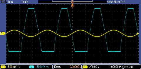
What is the maximum allowable input signal if the magnitude of the gain is increased to 10? Why?
If the magnitude of the gain is increased to 10, the maximum allowable input signal is 1/10 of the output signal. Since the expected output signal is known, which is 2.5V, the maximum allowable input signal is 250mV theoretically. In the simulation, the input amplitude is 250mV with a 2.5V offset. As you can see, it had already started clipping, which is possibly due to the resistance and capacitance in the equipments.
What is the point of the 0.01uF capacitors from VCC and VCM to ground?
-Are these values critical or could 0.1 uF, 1,000pF, 1uF, etc. capacitors be used?
If R1 and R2 were to be much larger, VCM will increase as well since the bias current is a constant value. To determine the VCM, you multiply the bias current with R1 and R2 in parallel. If R1 and R2 were to be in the 1k-100k range, VCM would be less than 1mV, which would not make too much of a difference in offset voltage. If R1 and R2 were to be 100MEG range, then VCM will be around 1V causing the offset voltage to increase . If VCM becomes too high, then the output will clip because it will exceed the voltage limit. The input offset current is the difference between the two bias currents from the op-amp because the two terminals do not necessarily have the same currents flowing.
Explain how the following circuit can be used to measure the op-amp's offset voltage.
-Note that if the output voltage is precisely the same as VCM then the op-amp has no offset voltage (this is very possible).
-To measure small offset voltages increase the gain by increasing RF to 100k or larger. Explain what is going on.

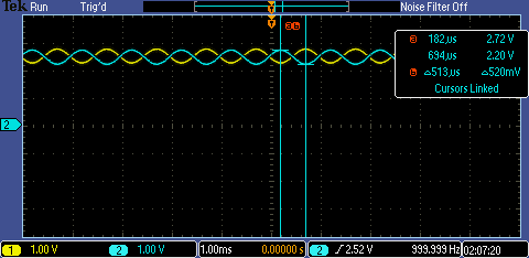
To measure the offset voltage, the difference between the output voltage and VCM are first calculated since VCM is considered the inputs for the op-amp. Those two voltages are probed on the oscilloscope and the difference between the voltages at its maximum is calculated. Once those difference are found, the gain is divided by the difference to find the offset voltage, which in this case is 20 (=Rf/Ri).
Measure the offset voltage of 4 different op-amps and compare them.
LM339

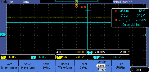
|Vout-VCM|/20 = |1.62-2.40|/20 = 39mV offset voltage
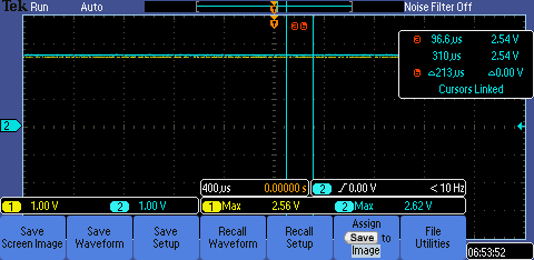
Based on the simulations of the 4 different op-amps, the TL081 op-amp had to the most offset voltage and the UA741 op-amp had the least.