Lab Project - EE 420L 

Authored by Sharyn Miyaji,

Email: miyajis@unlv.nevada.edu

Today's date: Wednesday,  May 3, 2017


Project description


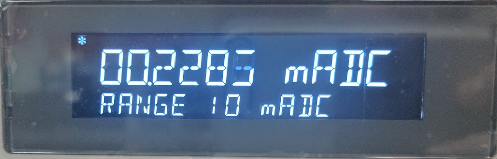
Design a transimpedance amplifier (TIA) using either the ZVN3306A or ZVP3306A (or both) MOSFETs and as many resistors and capacitors as you need with a gain of 30k. You should try to get as fast a design as possible driving a 10k load with as large of output swing as possible. AC coupling input and output is okay as long as your design can pass a 100 Hz input current. Your report, in html, should detail your design considerations, and measured results showing the TIA's performance. Note that this is the same project assigned last year so this year we will have one more constraint, that is, your design can draw no more, under quiescent conditions (no input signal), than 0.3 mA from a +9 V supply voltage (quiescent power consumption is less than 2.7 mW for any power supply you use).


Transimpedance Amplifier Design


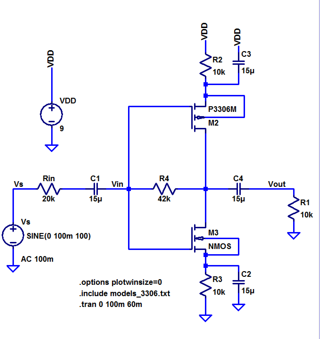
Below is the chosen design for the transimpedance amplifier, which is using the push-pull amplifier topology.  A push-pull amplifier is chosen for this project because of the 30k gain that is needed to meet the requirements since it can create a large amplification.   A resistor is connected in series with the input voltage source to create an AC current input source.   A big capacitor is also added in series to the input to block the DC voltages and allow the AC signals through.  A big capacitor is connected to the output of the push-pull amplifier on one end and the load resistor on the other end to again block the DC voltages from  going to the output.  The resistor and capacitor are in parallel and attached to the sources of both the NMOS and PMOS to limit the current flow through the circuit and prevent DC voltages from feeding back into the sources.  The resistor values were chosen based on trial and error and what was provided in the lab.


Schematic

http://cmosedu.com/jbaker/courses/ee420L/s17/students/miyajis/Project/TIA_schematic.PNG


The gain of the amplifier is based on the output voltage value divided by the current flowing through the resistor.  The simulation and measurements are shown below for comparison.
   

Simulations

Gain Simulation
(AC Analysis)
http://cmosedu.com/jbaker/courses/ee420L/s17/students/miyajis/Project/Gain_AC_analysis.PNG
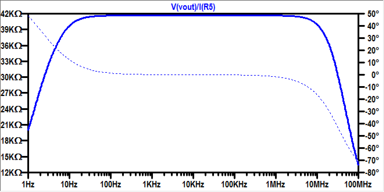
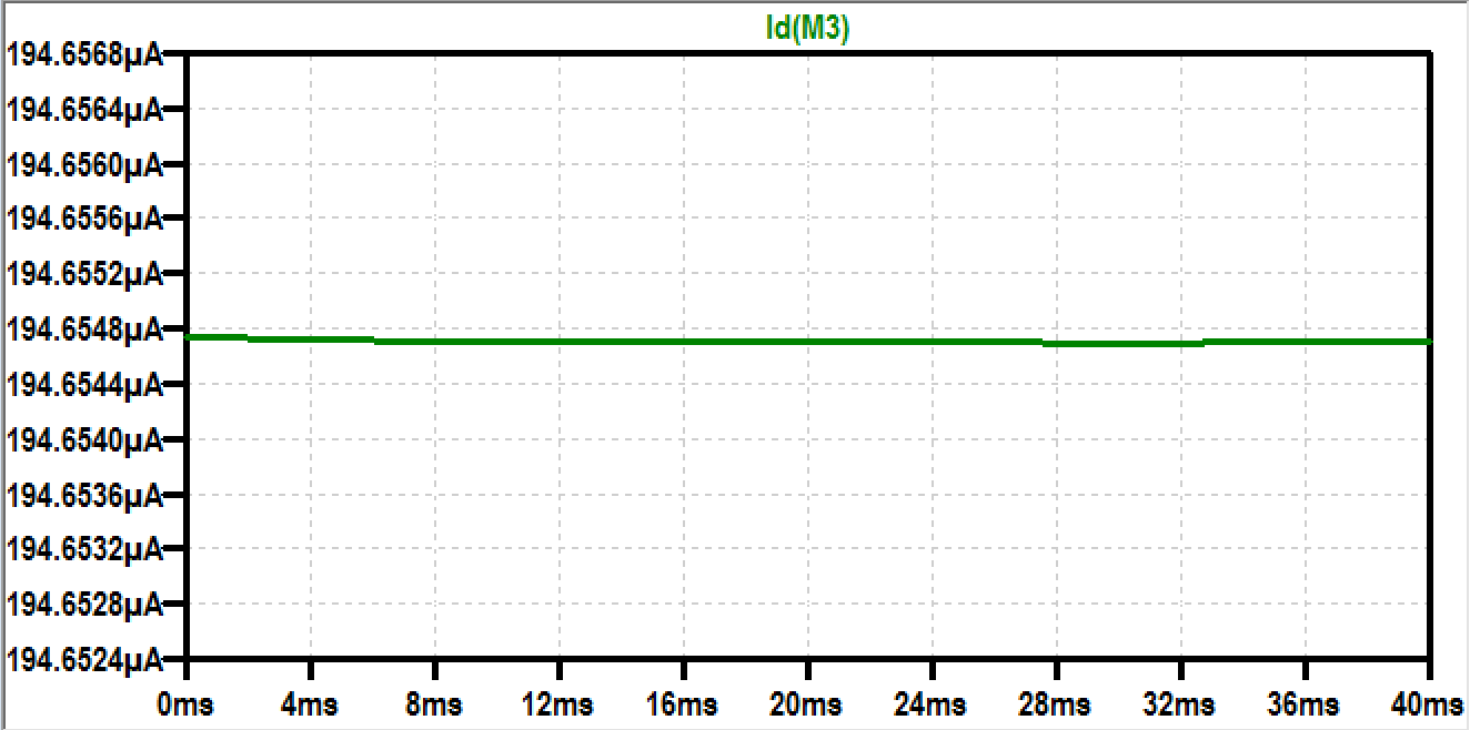
Gain Simulation (Transient)
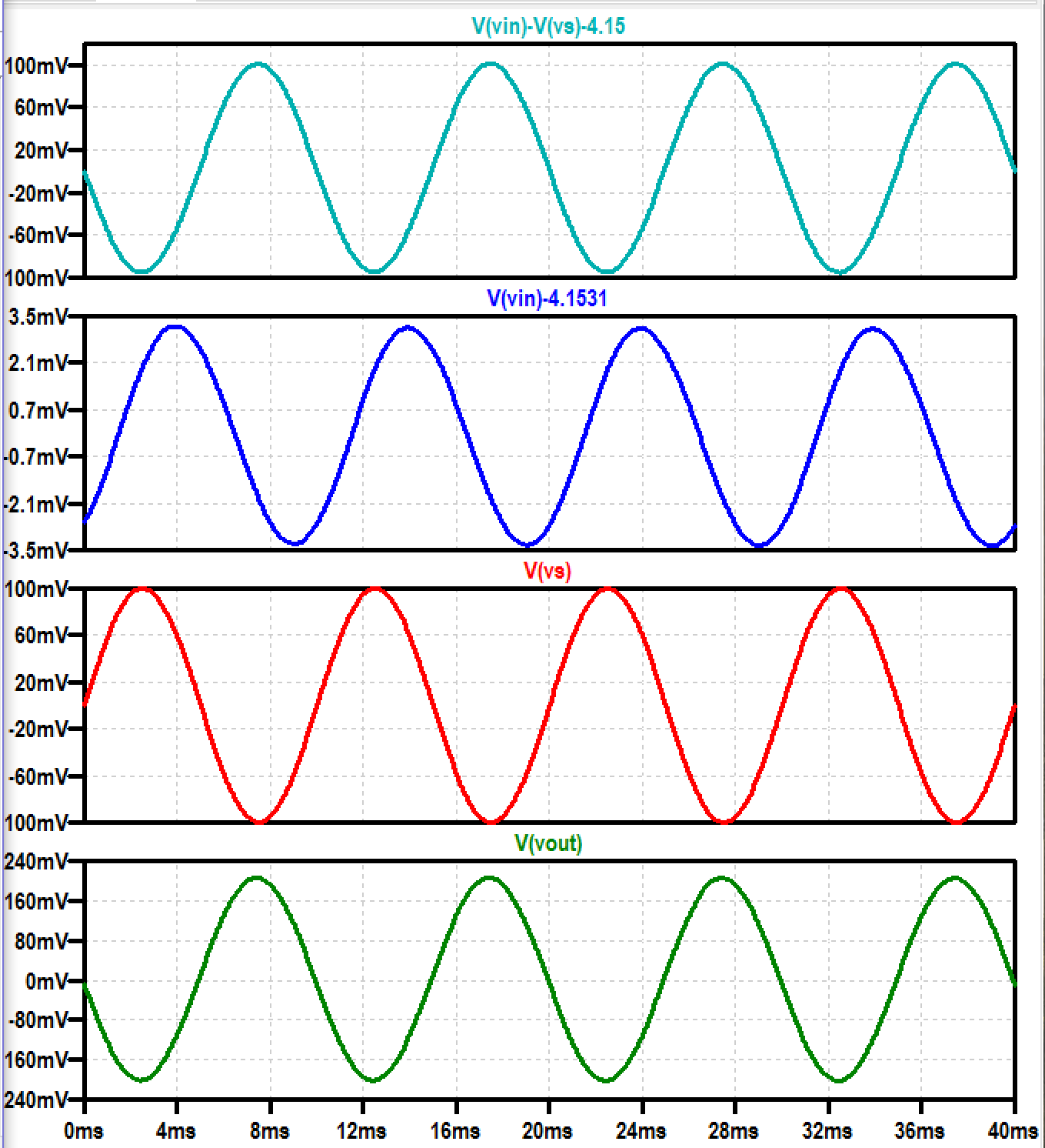
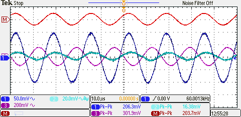
http://cmosedu.com/jbaker/courses/ee420L/s17/students/miyajis/Project/Gain_Voltages.PNG
Gain Measurementshttp://cmosedu.com/jbaker/courses/ee420L/s17/students/miyajis/Project/Gain.PNG


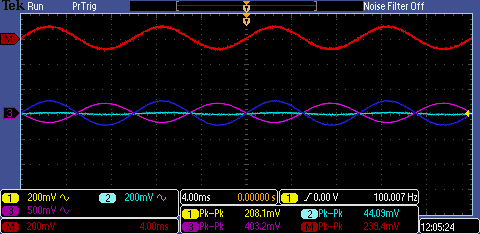
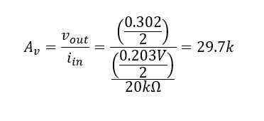
Based on the simulation, the gain is expected to be about 40k as seen in the AC analysis at 100Hz.  The voltages at three different nodes are simulated as well to compare the values measured on the oscilloscope.  The schematic is built on the breadboard and tested out to make measurements.  The following calculations are based on the measurements.


Gain Calculation

http://cmosedu.com/jbaker/courses/ee420L/s17/students/miyajis/Project/Gain_Calculation.PNG

   
The measured values are lower than what is expected.  The math function takes the difference between the AC source voltage and the AC input voltage, which may have not been accurate for the calculation.  Also the resistance and capacitance of the equipments may have been a factor for the gain being low.
   
The gain is tested out to see at what frequency the transimpedance amplifier will reach 30k gain for comparison.  Based on the AC simulation done earlier, the amplifier will reach a gain of 30k at about 40MHz.
       
http://cmosedu.com/jbaker/courses/ee420L/s17/students/miyajis/Project/Frequency.PNG
   
http://cmosedu.com/jbaker/courses/ee420L/s17/students/miyajis/Project/30kGain.PNG
   
As seen in the measurements, the frequency of the function generator is 60kHz which is not close to the simulation.  This may be due to how the schematic was laid out on the breadboard.
   
Output Swing
   
Next, the largest output swing is found by simulating and measuring the voltages by increasing the amplitude of the AC voltage source.
 
Input Amplitude = 620mVhttp://cmosedu.com/jbaker/courses/ee420L/s17/students/miyajis/Project/Output_Swing_Sim.PNG
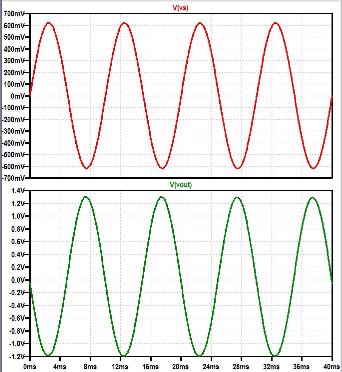
Input Amplitude = 640mVhttp://cmosedu.com/jbaker/courses/ee420L/s17/students/miyajis/Project/Output_Swing_Sim_Clipping.PNG
   
As seen in the simulations above, the amplifier starts to clip at about 640mV; therefore, the largest expected output swing is at am amplitude of 620mV.
   
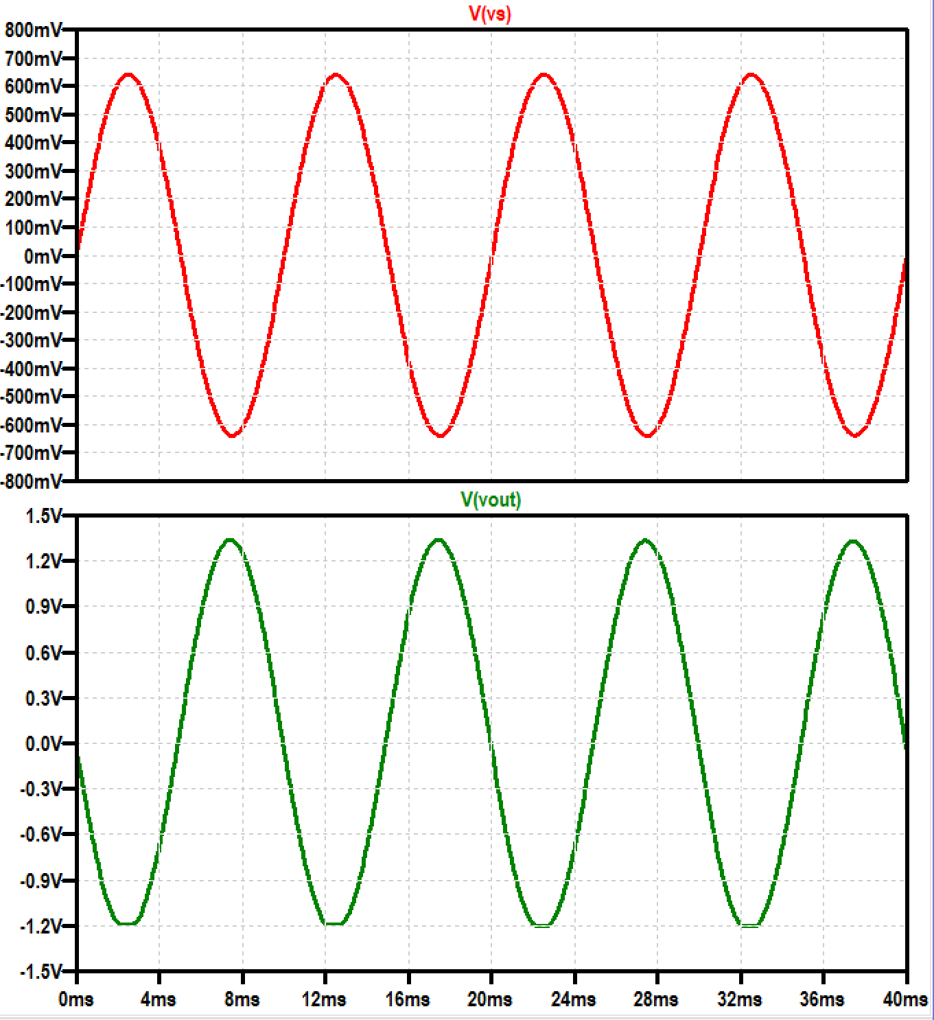
Input Amplitude = 1Vhttp://cmosedu.com/jbaker/courses/ee420L/s17/students/miyajis/Project/Output_Swing.PNG
Input Amplitude = 1.05V
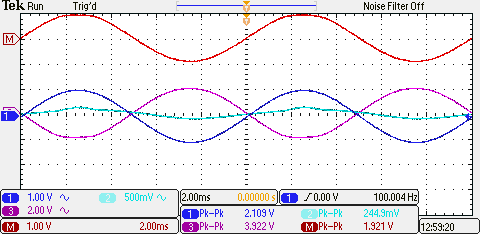
http://cmosedu.com/jbaker/courses/ee420L/s17/students/miyajis/Project/Output_Swing_Clipping.PNG
   
The measured output swing is higher than what was simulated.  This may be due to the equipment capacitance and resistance and the wiring on the breadboard.
   
Quiescent Power Consumption
   
The quiescent power consumption is measuring the current through the circuit without an input signal.  Since the maximum power consumption is 2.7mW and the voltage supply is fixed, the current flowing through the circuit can be 300uA at the maximum.
   
SimulatedMeasured
http://cmosedu.com/jbaker/courses/ee420L/s17/students/miyajis/Project/CurrentFlow.PNGhttp://cmosedu.com/jbaker/courses/ee420L/s17/students/miyajis/Project/CurrentFlow_Measured.PNG
   
As seen above, the current flowing through the circuit without an input signal is less than 300uA in both LTspice and the multimeter.  The difference is about 30uA which may have been cause by the resistance in the multimeter.


Return to Sharyn's EE420L Labs 

Return to EE 420L Labs