Lab Project - EE 420L
Authored
by Jeremy Garrod
5/3/2017
garrod@unlv.nevada.edu
Project Requirements
Design a transimpedance amplifier (TIA) using either the ZVN3306A or ZVP3306A (or both) MOSFETs and as many resistors and capacitors as you need with a gain of 30k.
You should try to get as fast a design as possible driving a 10k load
with as large of output swing as possible. AC coupling input and output
is okay as long as your design can pass a 100 Hz input current. Your
report, in html, should detail your design considerations, and measured results showing the TIA's performance. Note
that this is the same project assigned last year so this year we will
have one more constraint, that is, your design can draw no more, under
quiescent conditions (no input signal), than 0.3 mA from a +9 V supply
voltage (quiescent power consumption is less than 2.7 mW for any power
supply you use).
Design
A
transimpedance amplifier is an amplifier that converts an input current
into an output voltage. The design that I chose to implement is a
push-pull amplifier similar to the one seen below. This topology
naturally has a very large gain that is easily manipulated and accepts
a current as in input.

The
main issue with the topology above is that the DC current draw is
extremely large, my simulations showed a current draw of well over
100mA. This large amount of current of current is pushing the limits of
the transistors and would cause them to get very hot. Instead, the
modified version below is what was used due to the lower power draw.
There is still a large gain while the source resistors limit the amount
of current that the transistors can pull.The added large capacitors act
as a short for AC, which prevents any issues from arising from the
extra resistors added.

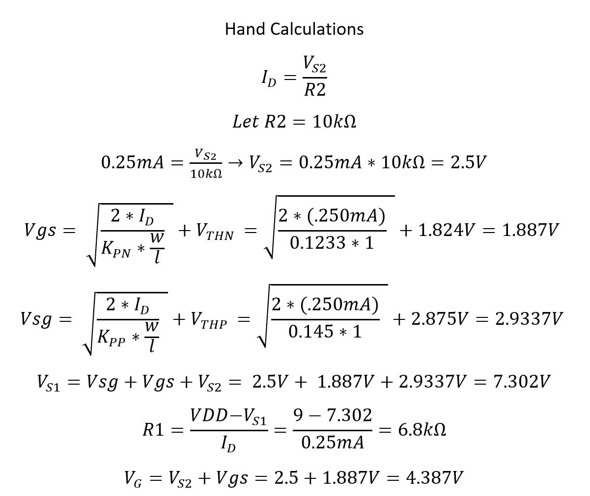
In
order to analyze the circuit for DC operation a 0.25mA current was
chosen in order to not go over the 0.3mA requirement. The Vsg and Vgs
of the PMOS and NMOS was then calculated. Next, a drain resistor was
chosen. I just wanted the source voltage of the NMOS to be a reasonable
value, so I chose a 10K resistor. After that was picked, the source
resistor of the PMOS could be calculated. The hand calculations are below.
To
get the gain of the circuit, multiple simulations were run and
analyzed. The gain of the circuit ended up being extremely close to the
value of the resistor Rf. The figures below are the various gains with
different feedback resistors. Even though the project requires a gain
of 30k, I went with a gain of 35k just to be safe. I did not any
imperfections in the real circuit to cause my gain to be under 30k
15k resistor

35k resistor

50k resistor

Now
that the gain is known, the next step is to test the output swing of
the amplifier. In order to test this, the current is raised until the
output voltage starts to clip. The value where it clips is the the
maximum and minimum voltage AC voltage that the amplifier can produce.

It
can be seen that the maximum voltage is roughly 3v and the minimum
voltage is roughly 2V. This can be adjusted by chaning the values of
the source resistors.
Experimental Results
The
experimental results may vary a little bit from my simulations and hand
calculations. I accidently grabbed a 6k resistor for the source of the
PMOS instead of a 6.8k. This lets a little more DC current flow in the
circuit, chaning the DC biasing by a little bit.
DC Biasing
In
order to make sure that my hand calculations were accurate and
that the DC operation of the circuit was correct I measured the voltage
at both of the transistor sources as well as the gates. It can be seen
below that the measured values are pretty close to the hand
calculations, the difference more than likely originates from the
different PMOS source resistor.
Measured DC Current = (9-7.2686)/6,000 = 280uA of current which is under the maxiumum of 300uA. The quiescent power consumption in this ciruit is 9V*280uA = 2.6mW.
Source of PMOS

Source of NMOS

Gate of both PMOS and NMOS

Measured gain at 100Hz.
In order to obtain the
gain, the voltage across the input resistor was measured. This divided
by the resistance gives the input current. The output voltage is then
divided by the input current. In the picture below, yellow is output
voltage, blue is input voltage, purple is voltage after the resistor,
and red is the voltage across the resistor

Gain = 2.720/(76mV/1000K) = 35,879
Measured output swing

The
bottom of the sine wave is starting to now get distorted. This means
that I am very close to the minumum voltage. The output swing pretty
close to what I had obtained in my simulations, however, I do not have
exact values.
Speed of the amplifier
To
measure the speed of the amplifier, the gain was calculated at various
frequencies. The plot below illustrates this and the table provides a
summary.

| Frequency (Hz) | Gain |
| 100 | 31,080 |
| 1k | 35,294 |
| 10k | 35,500 |
| 100k | 22,452 |
| 175k | 15,670 |
Conclusion
The
lab project was a success. A transimpedance amplifier was created that
drew a small amount of current while still having a large gain and a
respectable output swing. All of the requirements were met, although I
probably could have improved the output swing and lowere the current draw by adjusting the added resistors
Return to EE 420 Labs