Lab 8 Characterization of the CD4007 CMOS Transistor Array- EE 420L
Authored
by Jeremy Garrod
4/5/2017
garrod@unlv.nevada.edu
Pre-lab work
- Review the datasheet for the CD4007.pdf CMOS transistor array.
- Ensure
that you understand how the bodies of the NMOS are tied to pin 7 (VSS,
generally the lowest potential in the circuit, say ground) and that the
bodies of the PMOS are tied to pin 14 (VDD, generally the highest
potential in the circuit, say + 5V).
Lab Work
- Creation of Level 1 MOSFET Parameters
In
order to obtain the parameters of both the NMOS and the PMOS, a
1k resistor was placed in the source. The gate voltage was adjusted
until the voltage across the resistor starts to change, this is the
threshold voltage of the MOSGET. This resistor causes a voltage drop,
which can be measured and used to calculate the current. Once the
curernt is known, the source voltage can be measured, which allows the
gate-source and source-gate votlages to be calculated. Once all of that
has been completed, the square-law equation can be solved for the
transconductance, which along with the rest of the level 1 parameters,
can be found by plugging in all of the numbers above. The topologies
used along with the hand calculations are found below.


- Experimentally generate, for the NMOS device, plots of:
- ID v. VGS (0 < VGS < 3 V) with VDS = 3 V
- ID v. VDS (0 < VDS < 5 V) for VGS varying from 1 to 5 V in 1 V steps, and
- ID v. VGS (0 < VGS < 5 V) with VDS = 5 V for VSB varying from 0 to 3 V in 1 V steps.
While
an oscilloscope could be used to generate an IV plot, I have not done
that in a while and could not remember how to do it. Instead, I took
discrete measurements at various points, arranged it in a table, and
used EXCEL to generate the IV plots.
NMOS
1.

| VGS | ID(mA) |
| 0 | 0 |
| 0.5 | 0 |
| 1 | 0.0005 |
| 1.5 | 0.0898 |
| 2 | 0.4 |
| 2.5 | 0.858 |
| 3 | 1.518 |
2.
I
had some issues with the power supply, so I was not able to get a few
of the measurements. I ran my simulations with the corrected KP in
order to get a graph that was similar to mine and extrapolated the data
from there.

| VGS | 1 | 2 | 3 | 4 | 5 |
| VDS | | | | | |
| 1 | 0.005 | 0.2619 | 0.84 | 1.23 | 2.1 |
| 2 | 0.005 | 0.3521 | 1.16 | 2.15 | 3.65 |
| 3 | 0.005 | 0.3561 | 1.508 | 2.91 | 4.3 |
| 4 | 0.006 | 0.3589 | 1.520 | 3.244 | 4.791 |
| 5 | 0.007 | 0.3615 | 1.538 | 3.265 | 5.32 |
3.
I was not able to figure out how to do this experiment.
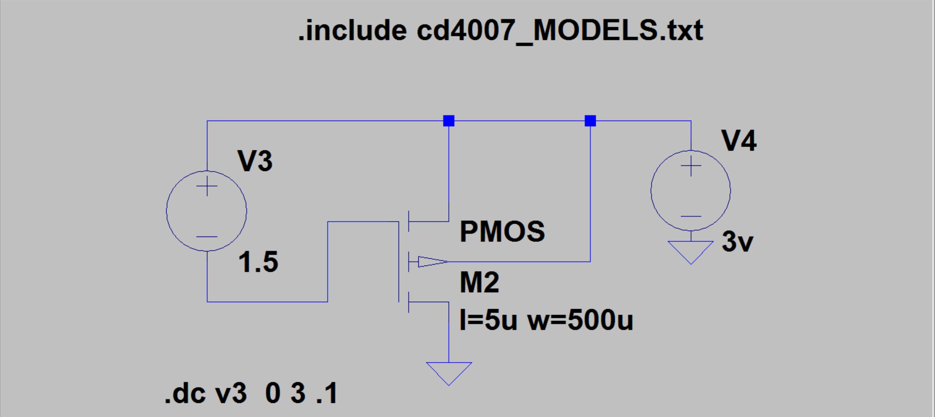
PMOS
1.

| VSG | ID(mA) |
| 0 | 0 |
| 0.5 | 0 |
| 1 | 0 |
| 1.5 | 0.0027 |
| 2 | 0.1322 |
| 2.5 | 0.4616 |
| 2.7 | 0.6889 |
| 2.8 | 0.8980 |
| 3 | 0.9324 |
2.
Just as with the NMOS, I
had some issues with the power supply. I was not able to get a few
of the measurements. I ran my simulations with the corrected KP in
order to get a graph that was similar to mine and extrapolated the data
from there.

| VGS | 1 | 2 | 3 | 4 | 5 |
| VDS | | | | | |
| 1 | 0 | 0 | 0 | 0.88793 | 1.1462 |
| 2 | 0 | 0.003 | 0115 | 1.2291 | 2.8136 |
| 3 | 0 | 0.003 | 0.469 | 1.8437 | 4.286 |
| 4 | 0 | 0.003 | 0.8397 | 2.3185 | 5.014 |
| 5 | 0 | 0.004 | 1.03 | 2.443 | 5.1615 |
3.
I did not able to figure out how to complete this experiment.
- Compare
the experimentally measured data above (the 3 plots) to
LTspice-generated data (again, 3 plots) and adjust your model
accordingly to get better matching.
NMOS


While
the shape is similar to my experimental plots, the values are quite a
ways off. In order to fix this, my value for KP needs to be adjusted. I
calculated a value of roughly 2.6uA/V^2, when in reality the KP should
be close to 5.5uA/V^2. The results of my adjusted parameters are below.
The new results are very close to my experimental values.


PMOS


The
shape and values are fairly close with a similar shape. The KP value
that I calculated is a little bit too high. A KP of around 9uA/V^2
gives me a waveform that is closer to what I measured in the lab.


- Experimentally,
similar to what is seen on the datasheet (AC test circuits seen on page
3 of the datasheet), measure the delay of an inverter using these
devices (remember the loading of the scope probe is around 15 pF and
there is other stray capacitance, say another 10 pF).
- Using
your model simulate the delay of the inverter and compare to measured
results. Adjust your SPICE model to get better matching between the
experimental data and the measured data.


I
could not figure out what I was doing wrong on this part. I built the
circuit using all three of the AC test circuits and I could not get any
of them to work. The waveform below is what I kept getting as an
output. I followed the wires multple times and double checked my
circuit. Nothing seemed to work. The circuit did not invert and had a
lot of noise on the output.


In
the simulations, I get a rise time of 28ns and a fall time of
30.9ns. These times are well within the values stated on the data
sheet. These values are with the adjusted KP values from the experiment
before.
Return to EE 420 Labs