Lab 6 Single-stage transistor amplifiers
Authored
by Jeremy Garrod
3/22/2017
garrod@unlv.nevada.edu
Pre-Lab work
- This lab will utilize the ZVN3306A and ZVP3306A MOSFETs.
- Review these datasheets and become familiar with these transistors.
- Verify that the simulations seen in lab6_sims.zip reasonably model the behavior of the transistors' ID v. VGS, ID v. VDS, and gm v. VGS curves.
- Finally, watch the video single_stage_amps and review single_stage_amps.pdf
Lab Work
- Below are schematics for NMOS and PMOS source followers amplifiers (also known as common-drain amplifiers).
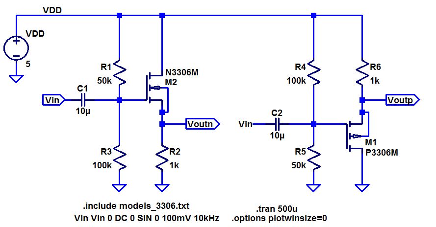
- In your lab report discuss the operation of these circuits
In
common-drain amplifiers, the input is on the gate while the output is
on the source. The drain is used for both the input and the output,
which is where it got its name from. The resistors that are connected
to the gate are used as a voltage divider in order bias the circuit to
a desired state. The DC input voltage determines the amount of DC
current which is flowing through the circuit, which in turn controls
the transconductance (gm) of the transistor. As Vin gets larger, it
turns the transistor on more, which causes the current to go up,
causing Vout to go up. With the above schematics, the input resistance
is determined by the resistors attached to the gate and the output
resistance is the resistance of the load in parallel with the
resistance looking into the source.


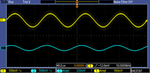
The
DC values were subtracted out of the waveforms in order to show the AC
gain. While neither of them are exactly 100mV, they are very close which confirms the hand calculations below.
- Hand
calculate, and then verify your hand calculations with experimentation
and simulations, the gains and the input and output
resistances ensuring that your test signals are at a high enough
frequency that the caps have negligible impedance but not so high that
the gain is dropping off.
- If
you build this circuit using electrolitic capacitors, assuming the
input AC signal swings around ground, put the "+" terminal of the cap
on the gate of the MOSFET. Please indicate, in your lab report, that
you understand why the capacitor is connected this way.
I
did not use any electolytic capacitors in my circuits. I could not find
a 10uF capacitor, nor any values that would add up to it. Instead, I
used a 12uF ceramic capacitor. However, if I did use an electrolytic
capacitor, the "+" would have had to have gone on the gate since the
"-" side of the capacitor is DC ground, the gate has a higher DC
voltage which is where the "+" side of an electrolytic capacitor goes.
If placed the wrong way, the capacitor would explode.


- In your lab report discuss, in your own words, how to measure the input resistance and output resistance.
The
input resistance is just the resistance of the two parallel resistors
on the gate. In order to experimentally measure that, you start by
putting a resistor that is close to the value that was calculated in
series with the input resistance. When the new resistor is added, it
creates a voltage divider between the new resistor and the input
resistance. If the new resistor is a match to the input
resistance, the voltage going into the gate now be half of the original
voltage. If it is not half, the input resistance can be solved for by
using the voltage divider equation as all of the other variables are
now known. The simulated results from this method can be seen
below for an input resistance of 33k both PMOS and NMOS with a 51 Ohm
output resistance on the NMOS and an 87.92 Ohm output resistance on the
PMOS
The
output resistance is measured in a very similar way. A resistor that is
close to the value of the output resistance is put in parallel with the
output resistance. When meausured, magnitude of the gain should be half
of what was originally measured. If not, the actual output resistance
can now be solved for with the information at hand.


The measurements will be the gain of the circuit, the input resistance, and the output resistance respectively.
NMOS


This was the only measurement
that I did not use amplitude values for.
PMOS


Summary of common-drain amplifiers
| NMOS | Gain | Input
Resistance | Output
Resistance | PMOS | Gain | Input
Resistance | Output
Resistance |
| Calculated | 0.95 | 33.3k | 51.02 | | 0.913 | 33.3k | 87.92 |
| Simulated | 0.934 | 33k | 51 | | 0.858 | 33k | 87.92 |
| Measured | 1
| 33k | 118
| | 0.7 | 33k | 29.9 |
These
results seem a little far off for some of the values, especially for
the PMOS circuit. The gain is .7 instead of the theoretical .9 and the
output resistance was calculated to be 29.9 Ohms based on the
experiment results. I am assuming that I must have made a mistake with
my component values or I didn't calculate my real output resistances
correctly from the data.
- Below are two common-source amplifiers.
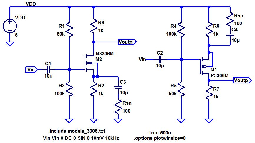
- Discuss the operation of these amplifiers in your lab report including both DC and AC operation.
In
common-source amplifiers, the input is on the gate of the transistor,
just as it was in the common-drain amplifier. However, the output is on
the drain instead of the source, with the source being common between
the input and output. Just as in the previous amplifier, the
resistors that are connected
to the gate are used as a voltage divider in order bias the circuit to
a desired state for DC. In AC, they are combined in parallel to form
the input resistance while the drain resistor determines the output
resistance. The
AC output gain is controlled by the resistor in the drain, the two
parallel resistors in the source, as well as the transconductance of
the transistor.
Gain


Input
Resistance
Output Resistance


- Hand calculate the gains and the input/output resistances.
- How does the source resistance, Rsn or Rsp, influence the gain.
Rsn
and Rsp affect the gain due to them being in the denominator of the
gain calculations, which can be seen below. Since the source resistance
is in parallel with another resistor, as the resistance goes up it
starts to make less and less of an impact. This would cause the gain to
go down, since the denominator of the equation wouuld start to go up.
The lower that the resistance goes, the smaller the denominator gets,
causing the gain to go up.


The
output resistance was handled the same exact way as the common-drain
amplifier. The images below, from left to right, are the gain, input
resistance, and output resistance.
NMOS


PMOS


Summary of common-source
amplifiers
| NMOS | Gain | Input
Resistance | Output
Resistance | PMOS | Gain | Input
Resistance | Output
Resistance |
| Calculated | -6.915 | 33k | 1k | | -5.391 | 33k | 1k |
| Simulated | 7 | 33k | 1k | | 5 | 33k | 1k |
| Measured | -5.59 | 33k | 1k | | -2.35 | 33k | 1k |
The
gains of both the NMOS and PMOS were a little bit lower than what was
calculated, with the PMOS being less than half of what was expected.
This could be caused by slight variations in the resistances due to the
allowed tolerance as well as fabrication differences. The input and
output resistance measurements were very good and produced results that
were nearly identical to the simulations.
- Below are two common-gate amplifiers
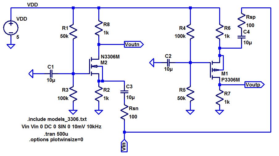
- Discuss the operation of these amplifiers in your lab report including both DC and AC operation.
For
DC, the two resistors on the gate act as a voltage divider, for VDD,
which allows the transistor to be in a desired state exactly like the
other amplifiers. The 10u capacitors prevent any DC current from
flowing in those directions, so all of the current flows through the
gate and source resistors along with the transistor. The DC current is
dictated by the square law equations. For AC, the capacitors act as a
short. The voltage is on the source, which creates a vgs or vsg
depending on which circuit is being looked at. That vgs causes a
current to flow and the AC input to be amplified according to equation
described in the hand calculations below. The amplification is
controlled by the transconductance of the transistor, the drain
resistor, and the source resistor.
Gain


Input Resistance
Output Resistance


- Hand calculate the gains and the input/output resistances.
- How does the source resistance, Rsn or Rsp, influence the gain.
Rsn
and Rsp are both in the denominator of the gain. When they both go
down, the denominator goes down which causes the gain to go up. When
they go up, the denominator gets larger which causes the gain to drop.
This is the same effect that is seen when you vary Rsp and Rsn of the
common-source amplifier.


The
schematics above were creatd and tested. The only issue with these
meaurements was that the scale on the oscilloscope was not quite low
enough, so the output voltages measures might be a slight bit off from
what they actually were.The images below, from left to right, are the
gain, input
resistance, and output resistance.
NMOS


PMOS


Summary of common-gate amplifiers
| NMOS | Gain | Input
Resistance | Output
Resistance | PMOS | Gain | Input
Resistance | Output
Resistance |
| Calculated | 6.506 | 153.7 | 1k | | 5.1 | 194.69 | 1k |
| Simulated | 7 | 153.7 | 1k | | 5 | 194.69 | 1k |
| Measured | 4 | 222.5
| 1k | | 1.36 | 231.5 | 1k |
The
output resistance was exactly the same as the simulations and
calculations. When putting a resistor of the calculated value in
parallel, the votlage dropped by half which is what was wanted. the
input resistances were both a little bit off though, with the NMOS
having a calculated input resistance that is 2/3 the value that was
obtained experimentally. Another issue is the gain of the PMOS. It
should have been close to 5, or atleast a value that is reasonable. The
gain of 1.36 that I obtained seems far too small for there to not have
been an error. - Below is a push-pull amplifier
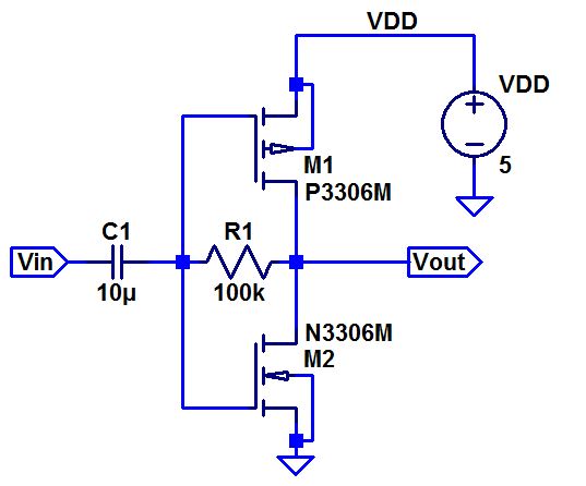
- Discuss the operation of this amplifier in your lab report including both DC and AC operation.
In
DC operation, both the transistors are gate-drain connected which pins
them in saturation. Other than that, I am not really too sure how this
circuit works in DC. For AC, the input current causes one of the two
transistors to shut off. If the current in positive, the gate of M1
goes up until the transistor turns off. The gate of M2 is also going
up, but that is turning the transistor on more and more. If the current
is is going the other way, the gate voltages will go down, shutting M2
off and turning M1 on.


- Hand calculate the gain of this amplifier.

- Do you expect this amplifier to be good at sourcing/sinking current? Why or why not?
This
circuit will be good at sourcing/sinking current. The PMOS will source
the current and the NMOS will sink the current, depending on what load
is attached. - What happens to the gain if the 100k resistor is replaced with a 510k resistor? Why?
Since
the resistor is by itself in the numerator of the gain equation, the
gain goes up linearly with that value. Since 510k is about 5 times
bigger than 100k, the gain should be about 5 times larger.
The lowest value that my function generator was able to output was 1mV, even though the oscilloscope has 1.6mV.


Summary of
Push-Pull amplifier
| 100k | Gain | 510k | Gain |
| Calculated | 2,916 | | 14,872 |
| Simulated | 2,000 | | 3,600 |
| Measured | 800 | | 1,480 |
While
my gain was large, it was very far away from what was expected. I am
not sure why this was the case, but I checked my circuit multiple times
to make sure that everything was properly connected and I had the
proper values for my resistors.
Return to EE 420 Labs