Lab 4 Op-amps II, gain-bandwidth product and slewing- EE 420L
Authored
by Jeremy Garrod
2/22/2017
garrod@unlv.nevada.edu
Pre-Lab Work
Watch the video op_amps_II, review op_amps_II.pdf (associated notes), and simulate the circuits in op_amps_II.zip.
Read the write-up seen below before coming to lab.
Lab Work
- Estimate, using the datasheet, the bandwidths for non-inverting op-amp topologies having gains of 1, 5, and 10.
The
gain-bandwidth product can be used to estimate the bandwidths for each
of the listed gains. The unity gain frequency is the frequency when the
gain is 1 or 0dB, given this information, the gain-bandwidth product
can be determined and then used to calculate the bandwidths of any
gain.

The
datasheet states that the gain-bandwidth product is 1.3MHz. Therefore
the following calculations represent the expected bandwidths of each
gain.
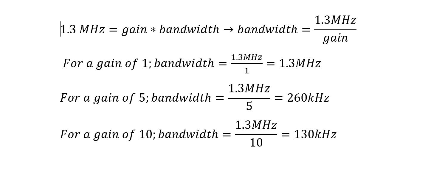
Hand calculations for bandwidths of non-inverting
topology
- Experimentally verify these estimates assuming a common-mode voltage of 2.5 V.
- Your
report should provide schematics of the topologies you are using for
experimental verification along with scope pictures/results.
- Associated comments should include reasons for any differences between your estimates and experimental results.
In
order to verify these estimates, two different measurements must be
made for each gain. The first measurement is at a low frequency in
order to get a baseline value for the output of the circuit. The next
measurement is at the -3dB point or .707 of the initial output value,
which will tell us the resulting bandwidth for each gain. The low
frequency that was used was 1kHz, due to the fact that I was almost
half way done before I realized I did not change the frequency that the
function generator was already set to, so I just kept going with it. At
the end of this experiment, there will be a table that summerizes
the values pictured below.
For a gain of 1:

Schematic for
non-inverting Op-amp with a gain of 1
Ideally, there would be no
resistor between VCM and the inverting terminal of the Op-amp. However,
there was an issue with the signal having some weird noise at the
bottom of the sine wave, so a 100k resistor was added to the circuit
which seemed to clean it up. I can't think of an explanation as to why,
it was just something that was discovered out of trial and error. The
only consequence I was able to find was that my VCM measured slightly
lower than the desired 2.5V.
I could not find the image of the
waveforms at 1kHz. However, the ouput voltage was fluctuating quite a
bit between about 90 and 130mV so I took the average and assumed that
the output was 110mV for the sake of simplicity. The image for the
inverting Op-amp with a gain of 1 had the same exact output, just in phase with the input, which can
be seen below.
One more note, the oscilloscope I was using did
not display the correct -3dB frequency the majority of the time. For
that reason, there will be an image of the function generator for each
incorrect frequency.

Waveform of the
non-inverting Op-amp with a gain of 1 at 1.25MHz

For a gain of 5:

Schematic for
non-inverting Op-amp with a gain of 5

Waveform of the non-inverting Op-amp with a gain of 5 at 1kHz

Waveform of the non-inverting Op-amp with a gain of 5 at 130kHz

For a gain of 10:

Schematic for non-inverting Op-amp with a gain of 10

Waveform of the non-inverting Op-amp with a gain of 10 at 1kHz

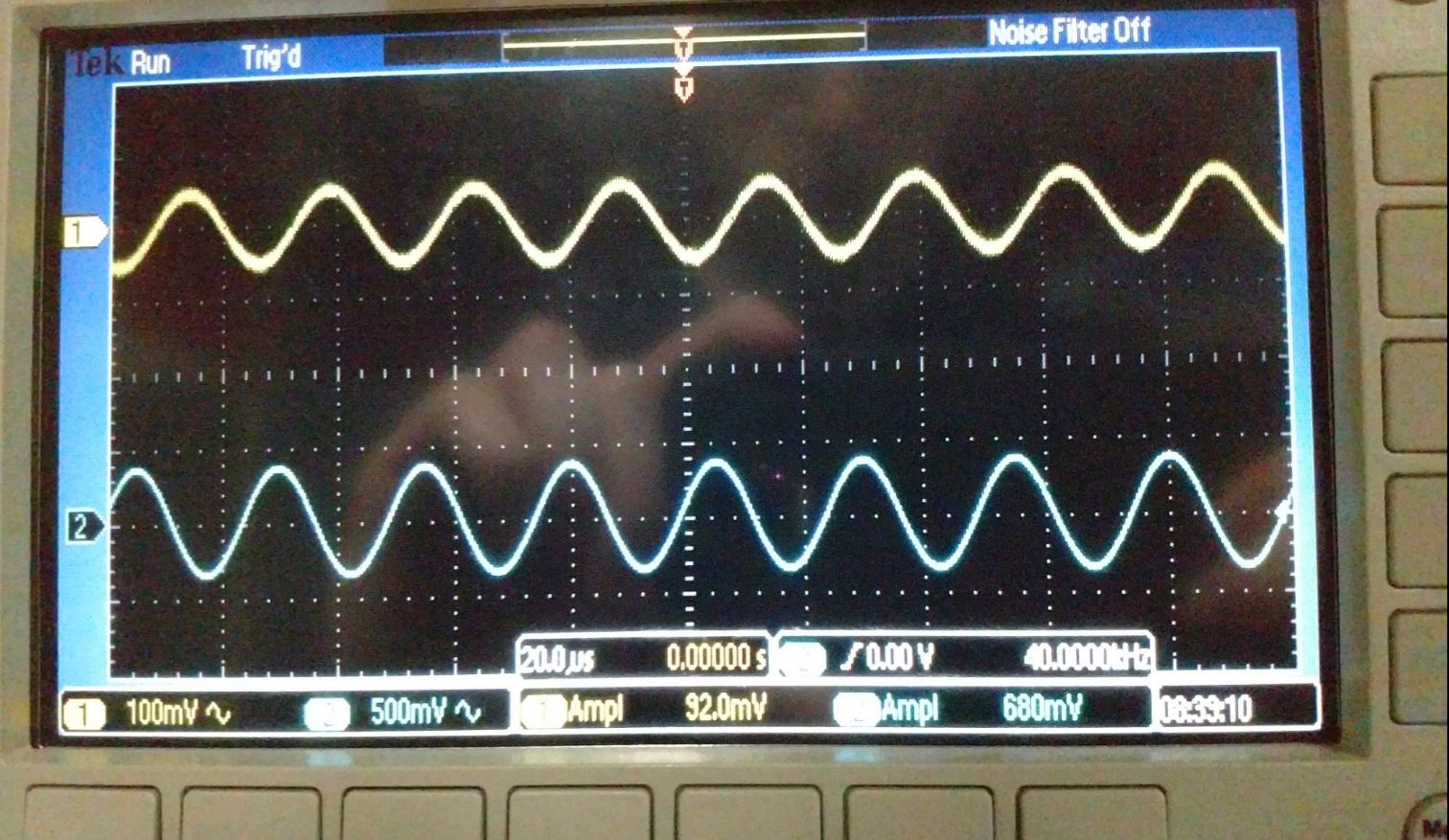
Waveform of the non-inverting Op-amp with a gain of 10 at 45kHz

| Gain | Vout | Measured Vout*.707 | Ideal Bandwidth | Measured Bandwidth |
| 1 | 110mV | 76mV | 1.3MHz | 1.25MHz |
| 5 | 456mV | 312mV | 260kHz | 130kHz |
| 10 | 960mV | 680mV | 130kHz | 45kHz |
The
measured bandwidth was very similar to the ideal bandwidth at lower
gains. The higher the gain became, the farther apart the measured
bandwidth was from the ideal that was calculated. This could be due to
many factors including process differences as well as human error in
the measurements. Another possibility is the fact that a different VCC
and peak voltage were used in this experiment than were used in the
datasheet. Lastly, my VCM was a little off, so that could have been a
contributing factor as well.
- Repeat these steps using the inverting op-amp topology having gains of -1, -5, and -10.

Hand calculations for inverting topology
For a gain of -1:
Similar to the non-inverting
topology, the output voltage for a gain of -1 at 1kHz varied between
about 90 and 130 so a value of 110mV was used.

Schematic for inverting Op-amp with a gain of -1

Waveform of
the inverting Op-amp with a gain of -1 at 1kHz

Waveform of
the inverting Op-amp with a gain of -1 at 575kHz

For a gain of -5:

Schematic
for inverting Op-amp with a gain of -5

Waveform of
the inverting Op-amp with a gain of -5 at 1kHz

Waveform of the inverting Op-amp with a gain of -5 at 95kHz
For a gain of -10:

Schematic for inverting
Op-amp with a gain of -10

Waveform of the inverting Op-amp with a gain of
-10 at 1kHz
Waveform of the inverting Op-amp with a gain of
-10 at 40kHz
| Gain | Vout | Measured Vout*.707 | Ideal Bandwidth | Measured Bandwidth |
| -1 | 110mV | 72mV | 650kHz | 575kHz |
| -5 | 488mV | 328mV | 217kHz | 95kHz |
| -10 | 960mV | 680mV | 118kHz | 40kHz |
The measured bandwidth was very similar to the ideal bandwidth at
lower gains. The higher the gain became, the farther apart the measured
bandwidth was from the ideal that was calculated. This could be due to
many factors including process differences as well as human error in
the measurements. Another possibility is the fact that a different VCC
and peak voltage were used in this experiment than were used in the data.
- Design
two circuits for measuring the slew-rate of the LM324. One circuit
should use a pulse input while the other should use a sinewave input.
- Provide comments to support your design decisions.
- Comment on any differences between your measurements and the datasheet’s specifications.
For
this design, I used the non-inverting topology from the beginning
of the lab. This allows for the rise of the ouput to be directly
compared to the input since they should be close in phase as well as
the close to the same amplitude. The slew rate is the change in voltage
over the change in time. In order to measure this, a signal at 300kHz
and a p-p of 500mV was put through the Op-amp. The time from 10% to 90%
of the signal strength was then measured. This allows the output to get
as linear as possible before looking at the values.
Schematic of circuit
used to calculate slew rate

Change
in voltage and time for square wave input

Change in voltage and time for sine wave input

Slew rate hand
calculations

LM324
datasheet slew rate
The slew rate that was measured was a little
bit lower than the slew rate listed on the datasheet. This could easily
caused by the fact that I used a different VCC along with non-ideal
VCM, process differences, etc. I also did not use a load to test my
circuit, where as they did in the datasheet. Other than those things, I am
not sure why my values would be as different as they are.
Return to EE 420 Labs