Lab 3 Op-Amps I, basic topologies, finite gain, and offset - EE 420L
Authored
by Jeremy Garrod
02/15/2017
Email: garrod@unlv.nevada.edu
Pre-Lab Work
Pre-lab work
Lab Work
- Knowing
the non-inverting input, Vp, is at the same potential as the inverting
input, Vm, (called the common-mode voltage, VCM) what are the maximum
and minimum allowable common-mode voltages?
- Support your answer with an entry from the electrical characteristics table in the datasheet.
The data sheet states that at +25ºC the minimum VCM is 0v and the maximum VCM is Vcc - 1.5V = 5V - 1.5V = 3.5V in the case of this experiment. The maximum Vcc that is allowed is +30V.

- What is a good estimate for the op-amp's open-loop gain?
- Support your answer with a plot from the datasheet and an entry from the electrical characteristics table.
The
data sheet states that the open-loop gain is 100V/mV which is a gain of
100,000 or 100dB. The second image below shows that the open-loop gain
is right around 100dB at 10Hz.


- What is a good estimate for the offset voltage?
- For worst case design what value would you use?
The
data sheet states that a typical offset voltage for the LM324 is 2mV,
so that is a good estimate of what to expect. For the worst case
design, the maximum offset should be used. While at +25ºC, which is room temperature,
the maximum offset voltage is 5mV the 9mV offset should be used when
designing for the worst case scenario. This accounts for extreme
temperatures as well as giving a nice buffer to the designer.

Build,
and test, the following circuit. Note that a precise value for the 5k
resistors isn't important. You can use 4.7k or 5.1k resistors.
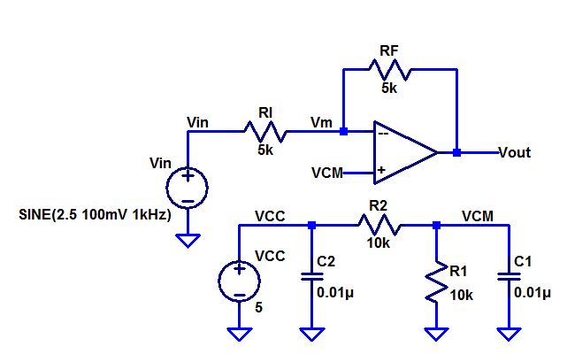
- What is the common-mode voltage, VCM? Does VCM change? Why or why not?
The
common-mode voltage is the voltage that is applied to both the inverting
and non-inverting terminals of the Op-Amp. It should be 2.5V in this
circuit due to the 2.5V offset on the sinusoidal source that is on the
inverting termincal as well the fact that there is a voltage divider
that outputs 2.5V to the non-inverting terminal. If everything was
ideal, the VCM should not change. The voltage divider and sinusoidal
source are both fixed and not variables. However, in reality there will
not be an exact match between terminals due to variations in each
source.

Voltage divider hand calculations

Output of voltage divider
- What is the ideal closed-loop gain?
Due to the inverting topology of the Op-Amp circuit, the ideal closed-loop gain is -1

Ideal Closed-Loop Gain Hand Calculations
- What is the output swing and what is it centered around?
- What happens if the input isn't centered around around VCM, that is, 2.5 V?
- Provide a detailed discussion illustrating that you understand what is going on.
The
output swing is the voltage range that is actually output by the
Op-Amp. In this experiment, the swing is roughly 200mV and is centered
around VCM which is 2.5V. Due to the inverting topology, the output
will have the same amplitude as the input but 180º out of phase. This
can be seen in an image below. If the input is not centered around VCM
then the output can possibly clip. Since the swing is both positive and
negative, if you go down too low you risk going under the 0V lower
limit and clipping. If you go too high then you risk going above the 5V
upper limit and clipping.

Input and output waveforms showing a gain of -1

Waveforms when input is centered around 0V
- What is the maximum allowable input signal amplitude? Why?
Since
the output swing is centered around 2.5V, the input signal amplitude
can't be larger than 2.5V or else it will go over the 5V Vcc+ and clip
as well as go under the 0V Vcc- and clip.
- What is the maximum allowable input signal if the magnitude of the gain is increased to 10? Why?
If
we are increasing the gain to 10, that means that the input voltage
will be multiplied by 10. In order to keep within the 2.5V input signal
boundary, the input signal can't be larger than 2.5V/10 or 250mV or
else it will be amplified past the supply voltage.
- What is the point of the 0.01 uF capacitors from VCC and VCM to ground?
- Are these values critical or could 0.1 uF, 1,000 pF, 1 uF, etc. capacitors be used?
These
capacitors are used to keep the DC voltage of VCM at a constant value.
If any changes were to occur with the power supply, the capacitors will
make up for the loss of voltage. They also filter out any AC noise that
may come from the power supply or other sources since they act as a
short to AC signals. This keeps a nice and clean DC signal going into
the inverting terminal of the Op-Amp. The capacitances should be fairly
large in order to act as a wire for AC signals. Other than that one
condition, the values do not matter.
- The data sheet shows that this op-amp has an input bias current that flows out of the op-amp's inputs of typically 20 nA.
- This current flows out of both the non-inverting and inverting inputs through the resistors connected to these inputs.
- Show how the operation of the circuit can be effected if, for example, R1 and R2, are much larger. Explain what is going on.
This
bias current flows through R1 and R2 which the bias current sees as
being in parallel. This current flow causes a a voltage drop, which
actually increases our VCM voltage. In this experiment, R1 and R2 were
both 10k. This would cause a voltage drop of 20nA * (10k||10k) = 0.1mV.
This is a tiny voltage, so adding it to VCM doesn't do much. However,
if the resistors were larger, such as 1MEG you would get a voltage drop
of 20nA * (1MEG||1MEG) which creates a drop of 10mV. Adding this larger
voltage to VCM would change the output of the circuit and possibly
cause clipping. Sadly, I did not get a picture of the output of the circuit with larger resistors.
- What is the input offset current? What does this term describe?
There
is an input bias current that flows out of both terminals. If they are
not equal, the difference is called the input offset current. For the LM324 Op-Amp, the input offset current can be seen in the image below.

Explain how the following circuit can be used to measure the op-amp's offset voltage.
- Note that if the output voltage is precisely the same as VCM then the op-amp has no offset voltage (this is very possible).
- To measure small offset voltages increase the gain by increasing RF to 100k or larger. Explain what is going on.
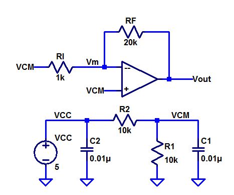
In
this circuit, the voltage divider provides the voltage to both
terminals of the Op-Amp. If it was an ideal Op-Amp, there would be no
current flow, which means that VCM and VM have the same voltage.
However, if there is an offset then Vm and VCM would not be equal,. The
offset of the Op-Amp would be added to VCM, making VM = VCM + Voffset.
This offset will then be amplified by the gain of the inverting
amplifier and added to the output voltage. So, in order to measure the
offset voltage, take the output voltage and subtract if from VCM and
then divide by the magnitude of the gain. For example, if the output
voltage was 2.4V and VCM was 2.5V with a gain of 20 the offset would be
(2.5V-2.4V)/20 = an offset of 5mV.
- Measure the offset voltage of 4 different op-amps and compare them.
In the folllowing images, the measured VCM will be on the left and the measured Vout will be on the right.


LM324
(2.4959V - 2.4940v)/20 = 95uV
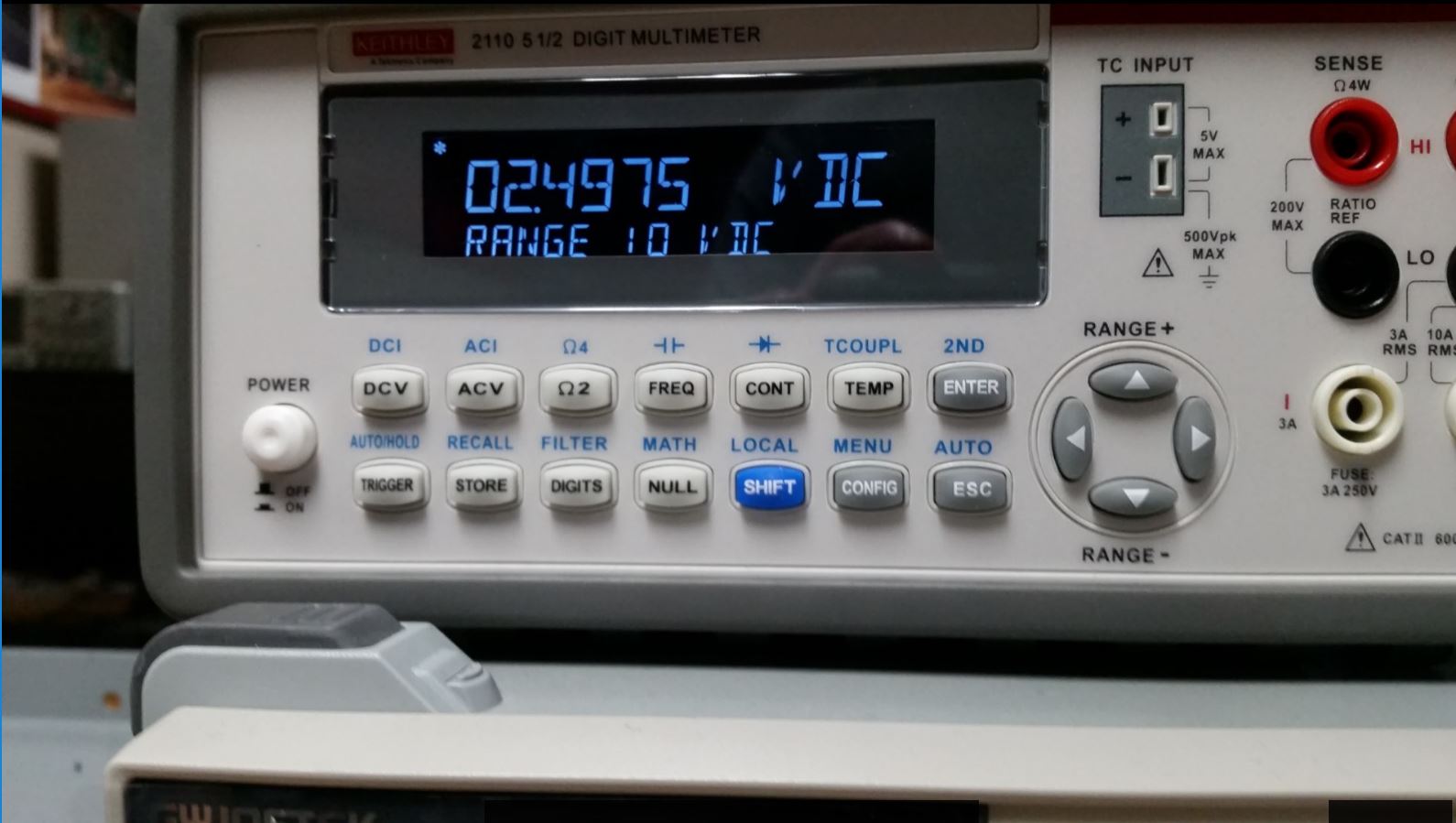

LM339
(2.4975V - 2.4922V)/20 = 265uV


LM348
(2.4999V - 2.5157V)/20 = -790uV


TL081
(2.3835V - 1.9123V)/20 = 23.6mV
Return to EE 420 labs