Project - EE 420L
Authored
by Tyler Ferreira,
ferret1@unlv.nevada.edu
May 2, 2017
Project - design a transimpedance amplifier (TIA) using either the ZVN3306A or ZVP3306A (or both) MOSFETs and as many resistors and capacitors as you need with a gain of 30k.
You should try to get as fast a design as possible driving a 10k load
with as large of output swing as possible. AC coupling input and output
is okay as long as your design can pass a 100 Hz input current. Your
report, in html, should detail your design considerations, and measured results showing the TIA's performance.Note
that this is the same project assigned last year so this year we will
have one more constraint, that is, your design can draw no more, under
quiescent conditions (no input signal), than 0.3 mA from a +9 V supply
voltage (quiescent power consumption is less than 2.7 mW for any power
supply you use). Your report is due at the beginning of lab on Wednesday, May 3. Access to your CMOSedu.com accounts will be removed at this time.
I decided to design my transimpedance amplifier around the push-pull amplifier topology.
Here is the schematic I built in LTspice and will implement on to my breadboard:
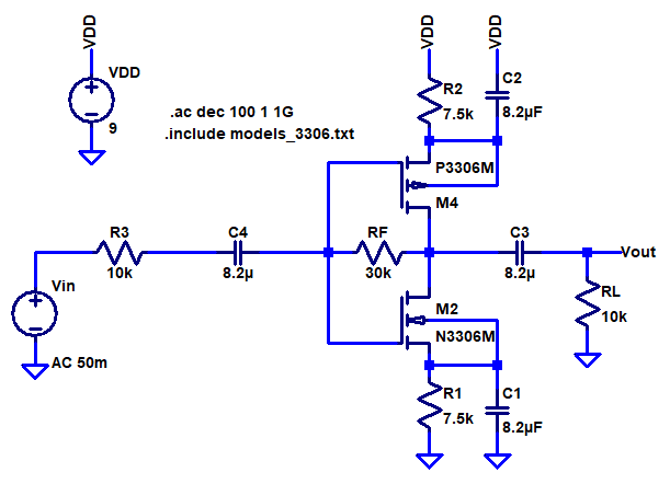
The
voltage source in series with a resistor on the input is to generate an
input current for testing. I will connect 2 scope probes across this
resistor to measure the current through it.
I
will use resistors in parallel with capacitors on the sources to limit
the current flow through the transistors to 0.3mA and to ground the
sources during AC analysis.
By doing this I will be able to obtain a quiescent power consumption of less than 2.7mW without really affecting my gain.
I
will design my circuit to have a DC drain current close to the maximum
allowable current of 0.3mA in order to have a larger output swing.
Below is my thought process and hand calculations for finding the required feedback resistance to obtain a gain of 30k.
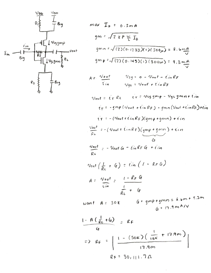
To
obtain a gain of 30k I will need a resistor of around 30,111 ohms. The
closest resistance I could get in the lab was a 30k resistor. I will
test this and compare with my LTspice simulations.
| LTspice Simulation | Experimental |
 |  |
I
built my schematic in LTspice using the values of the real components I
was able to obtain in the lab. These values worked well for my project
as they provided enough gain, speed, and a low enough quiescent power
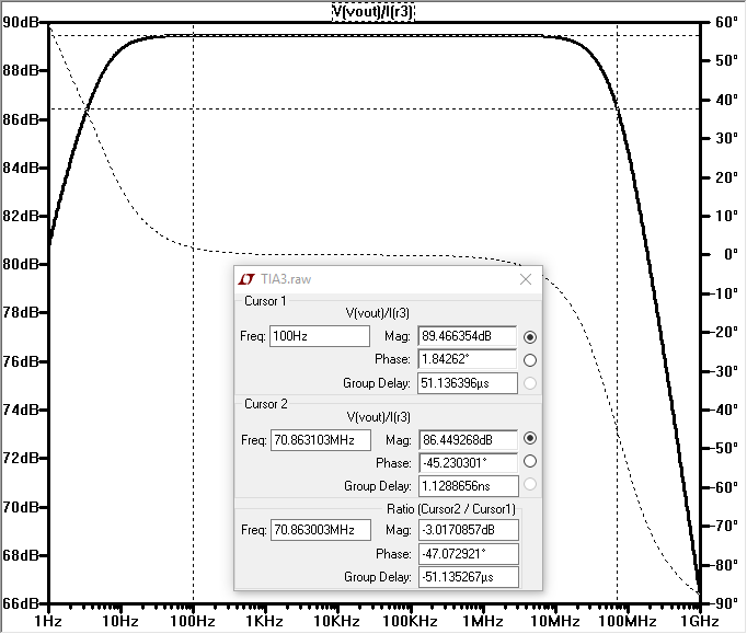
consumption. In my LTspice simulation I am obtaining a gain of 89.46dB
at 100Hz and my gain starts to roll off at 70.8MHz. I have obtained a
pretty fast design but my gain is not quite 30k in my simulation.
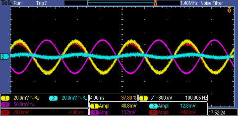
Testing this design on my breadboard I obtained the following gain:
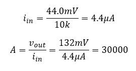
Obtained
by dividing the difference in voltage across the input resistor by the
resistance to find input current. Then by dividing my output voltage by
this current I obtain the transimpedance gain of my TIA.
In my
experimental tests I obtained a gain of exactly 30k at 100Hz. I will
now test the speed of my design by varying the frequency on the
function generator and creating a spreadsheet to see when the gain
starts to drop off.
Table of my results:
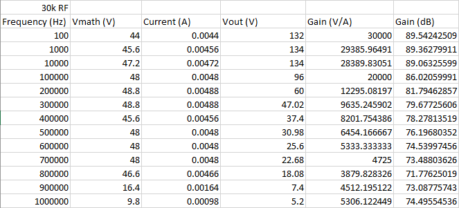
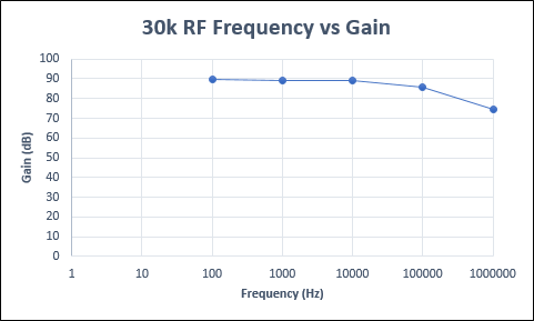
I plotted my data in a bode plot and can see that my gain begins to drop off around 100kHz to 1MHz.
In my LTspice simulations my gain wasn't dropping off until around 70MHz but on my breadboard I am rolling off at around 100kHz.
This is expected since my circuit is not ideal as it is modeled in spice.
I
will now show the output swing of my design in LTspice and
experimentally. I will simply increase the input current until my
output begins to clip.
In LTspice I will input a large amplitude sine wave and run a transient analysis to observe the clipping.
The points at which my output voltage clips will indicate my output swing.
| LTspice | Experimental |
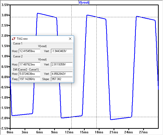 | 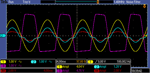 |
Table comparing my values:
| LTspice | Experimental |
| +Voltage | 2.91V | 2.8V |
| -Voltage | -1.94V | -2.0V |
| Total Swing | 4.85V | 4.8V |
My experimental results are very similar to my simulated results.
I will test the quiescent power consumption of my design by connecting
the power supply to my multimeter to measure the current flowing
through it.
I will not have an input signal flowing into my circuit while performing this test.
Image of my multimeter measuring the current supply from my 9V power supply:
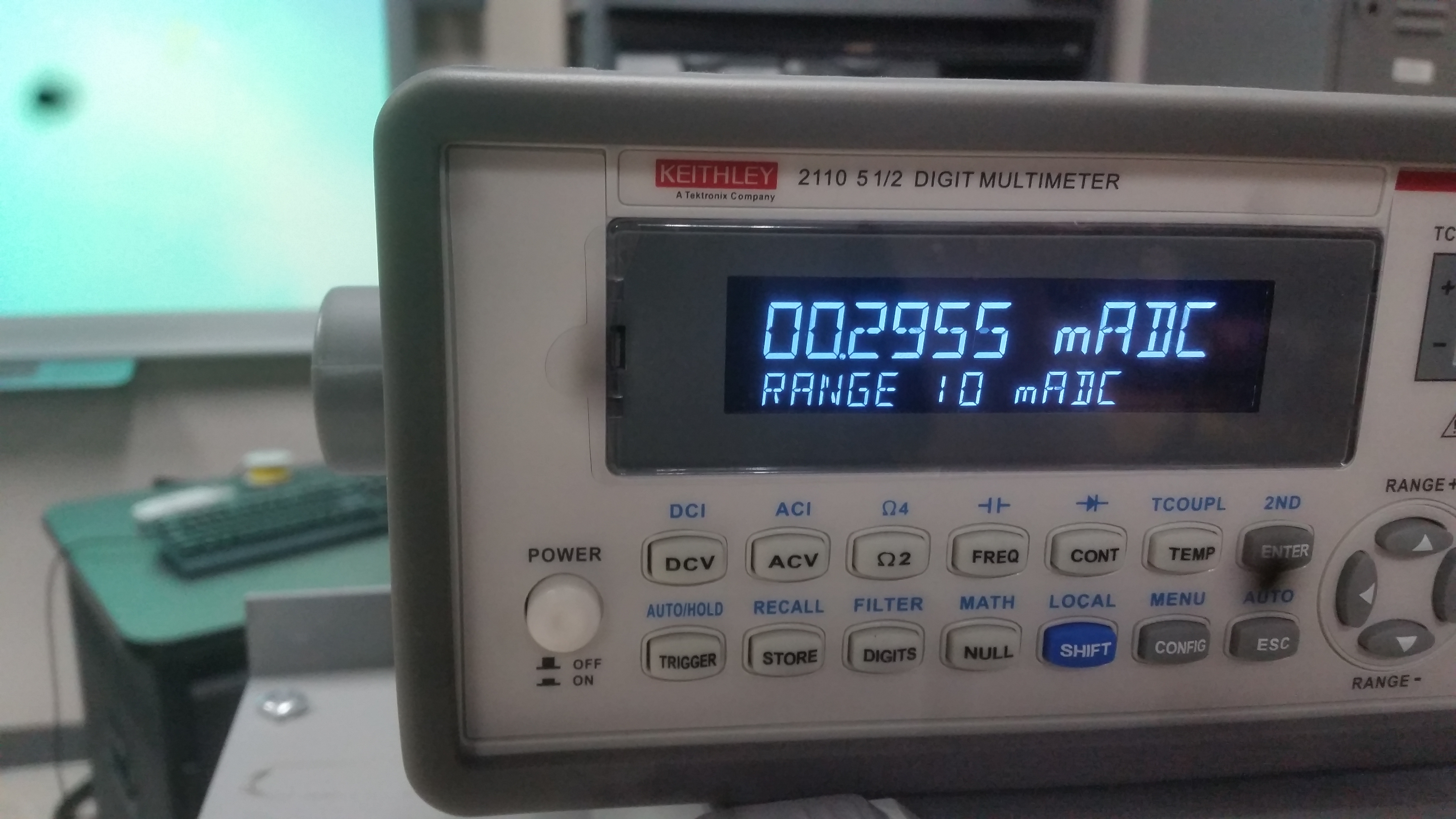
My current supply is 0.2955mA which gives me a quiescent power consumption of 2.65mW.
Conclusion:
My
transimpedance amplfier design was able to satisfy the design
specifications of the project. While driving a 10k load I obtained a
gain of 30k at 100Hz, my gain rolled off at 70.8MHz in my simulations
and around 100kHz - 1MHz in my breadboard design, and I was able to
have a quiescent power consumption of less than 2.7mW.
I will backup my work on to my OneDrive and my desktop:
Return to the directory listing of my labs
Return to the directory listing of students in EE 420L, Spring 2017
Return to the EE 420L, Spring 2017 webpage