EE 420L Engineering Electronics II - Lab 1
5/4/16
Design Considerations
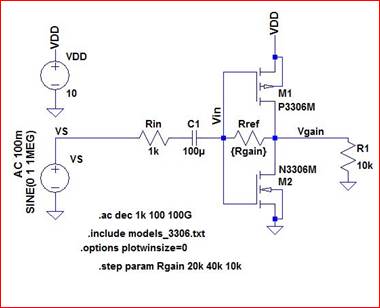
A trans-impedance amplifier (TIA) converts a current input to a voltage
output. The design for selected for this project is a simple push-pull
amplifier. The topology used for this project is seen in the figure below.
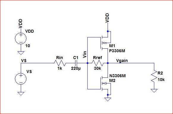
This choice was made for simplicity and the efficiency inherent in
a push-pull design, as well as for time management considerations. The
characteristics of a push-pull amplifier include low distortion, high
efficiency and high output power. However, the main reasons for selecting this
topology are the push-pull amplifier has a large gain that is linearly related
to the feedback resistor, Rref , seen in the above circuit, along with a high input
impedance and low output impedance. This makes the design suitable for driving
low impedance loads, but unfortunately results in a high current draw at no load.
The push-pull amplifier drives a current in two directions through
a load. This means each transistor is conducting for slightly more than a half
cycle of conduction, but as the waveform crosses zero and each transistor is
conducting, the effects of each transistor operating cancel each other
out. The PMOS and NMOS are used to
source current through the load and sink current from the load. The input and
output of the circuit are connected via Rref,
allowing the circuit to be self-biased with no DC current flow in the
transistors. The 1kΩ resistor
functions as a method of creating a current input for the TIA.
Theoretical
Gain Calculation
The ZVN3306A and ZVP3306A transistors were previously used in
laboratory experiments six and seven. Referring to Lab7, the experimentally
determined transconductance of the NMOS is 19.0mA/V
and the PMOS is 13.3mA/V versus the Spice Model values of 18.3mA/V for the NMOS
and 10.7mA/V for the PMOS. The gain of the push-pull amplifier is displayed
below.
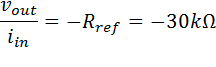
Simulated
Gain
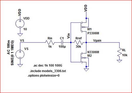
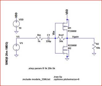
The simulations for the gain of the push-pull amplifier are seen
below. The circuit is displayed on the left with the 30kΩ gain displayed
on the right. Notice the gain is 180![]() out of phase, thus confirming
the negative gain. Also, notice a 10VDD bias is used for the circuit. This was
done to supply enough current to drive the 10kΩ resistor with the
tradeoff of a high current draw at no-load conditions. To counter high
temperatures in the transistors due to the high current, approximately 150mA,
heat sinks were incorporated into the circuit.
out of phase, thus confirming
the negative gain. Also, notice a 10VDD bias is used for the circuit. This was
done to supply enough current to drive the 10kΩ resistor with the
tradeoff of a high current draw at no-load conditions. To counter high
temperatures in the transistors due to the high current, approximately 150mA,
heat sinks were incorporated into the circuit.
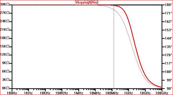
Notice the simplicity of the design allows that Rref essentially establishes the gain. Sweeping Rref from 20kΩ to 40 kΩ in 10 kΩ
steps shows how the gain changes linearly with Rref.
The waveform displays the gains at each step, in order, top to bottom.
Experimental
Gain No-Load
Testing the gain in the laboratory proved to be more challenging
than anticipated with such a simple design. The main reasons for this were poor
circuit design and an issue with coupling capacitors, as well as a faulty
oscilloscope probe. The initial design was spread out too far across the board,
as opposed to close and tight. This introduced noise into the circuit and made
obtaining readable signals difficult. After changing the faulty probe,
rebuilding the circuit, and connecting DC biasing directly from the source, as
opposed to through the board rails, the circuit operated almost as intended.
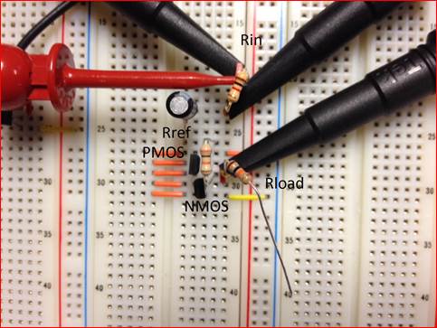
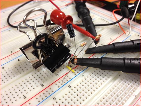
To begin, an image of the circuit is displayed below.
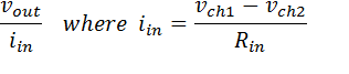
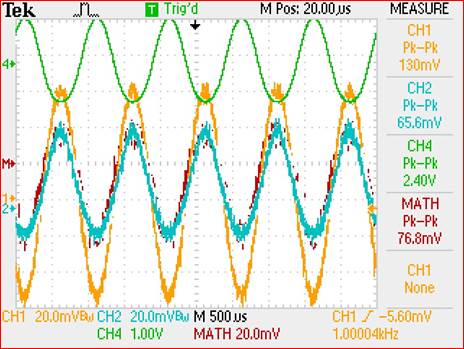
To measure the no-load gain of the circuit, three oscilloscope
probes were used, along with the math function. Probes on channels 1 and 2 were
used to measure the voltage on either side of the 1kΩ resistor. The math
function was used to determine the difference between the channel
1 and channel 2 peak to peak voltages. Finally, a probe on channel 4 measured
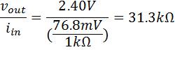
the output voltage. The gain is then calculated using the following equations:
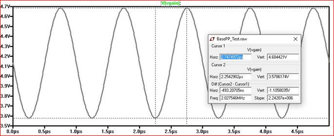
The oscilloscope image below displays the experimental results for
the 30kΩ resistor.
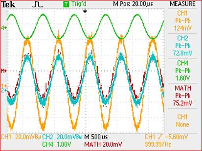
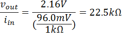
However, using the 30kΩ resistor results in the following
gain:
The first attempt to rectify this issue was to try a
larger Rref . Replacing the 30kΩ resistor with a 42kΩ
resistor resulted in the following waveform:
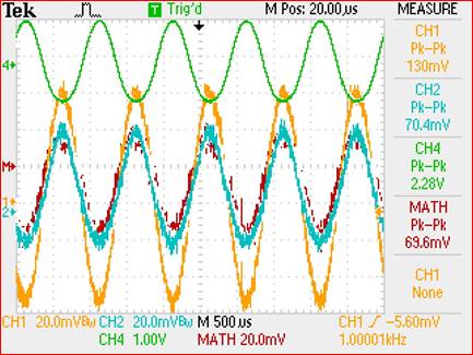
Repeating the gain calculation now resulted in the following:
This result was deemed acceptable due to the variations in the
measured values on the oscilloscope.
One of the drawbacks to using this large of a DC source is the
heating that occurs in the transistors due to the high current. For the
experiment, two binder clips were used as heat sinks to keep the transistors
from overheating. These functioned quite well and served to allow the design to
run for an extended duration of time without overheating issues. This is seen
in the image below.
Experimental
Gain with 10kΩLoad
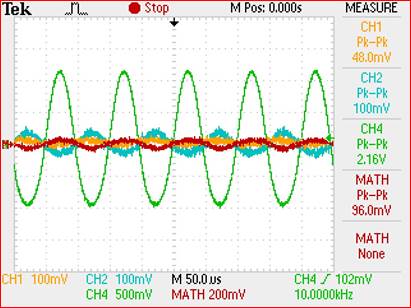
The initial design consideration included plans to include a
source follower stage in order to add a low impedance output stage that would
allow the amplifier to drive the required load. However, before attempting to
model and build this stage, the 10kΩ load was placed at the output of the
push-pull amplifier to see if it would drive the load. The resulting waveform
is displayed below.
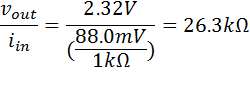
Performing the gain calculation gain resulted in the following:
Thus, the push-pull amplifier can drive the 10kΩ load. To
see if this amplifier could drive anything smaller than this load, a 5kΩ
load and an 8kΩ load were tested, the 5kΩ load first. The resulting
waveform for the 5kΩ load is displayed below. The 8kΩ waveform was
nearly identical to the 5kΩ waveform, thus it was omitted.
The gain calculation for the 5kΩ load results in the
following:
Clearly, the 5kΩ is too small for the push-pull amplifier to
drive without an additional stage, but the amplifier was able to drive the 10kΩ
load.
Passing a 100Hz Signal
The design needed to be able to pass a 100Hz signal. This resulted
in the need for a capacitor large enough to allow for this speed. A 220uF
capacitor was selected to provide ample capacitance to allow this signal to
pass. The resulting waveform is displayed below.
The gain using the 100MHz signal was calculated as follows:
Again, the fluctuations in the measured values on the oscilloscope
showed the gain in the neighborhood of 30kΩ.
Output
Swing
The output swing of the simulation showed an output swing of 1.1V
for this design with 10VDD and a 20mV amplitude sinusoidal input. The results
of the simulation are displayed below.
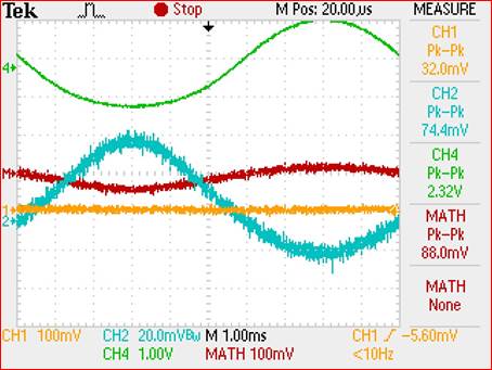
Measuring the output swing in the laboratory under the same
conditions results in the following waveform:
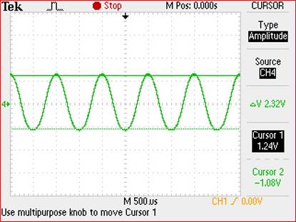
The output swing is approximately 2.32V.
Conclusion
The transimpedance amplifier design was
simple, yet performed as intended. The TIA design has a 30kΩ gain and can
drive a 10kΩ load and pass a 100Hz signal. Despite the design functioning
as intended, time constraints presented a challenge in designing and
characterizing a more unique and efficient TIA that would meet all project
specifications. This project is not up to the standards of work I aspire to
achieve, however this is the result presented for evaluation. Lastly, the
laboratory project presented an opportunity to utilize many of the skills
developed and refined in the laboratory this semester and created yet another
opportunity to practice fundamental analog design techniques.
Return to
Monahan Lab Report Directory
Return to EE420L
Spring 2016 Student Directory