EE 420L Engineering Electronics II - Lab 9
4/20/16
Pre-lab
work
This lab will use
the level=1 MOSFET model created in lab 8 and, again, the MOSFETs in the
CD4007.pdf CMOS transistor array.
- Design and simulate the
operation of a BMR that biases the NMOS devices so that they have a gm of 20 uA/V
- Use a simple (big) resistor to
VDD for the start-up circuit (explain how the addition of a resistor
ensures start-up).
- When the BMR is operating the
current in the big resistor should be much smaller than the current
flowing in each branch of the BMR
- Write-up, similar to a homework
assignment, your design calculations and simulation results. (This will
count as the pre-lab quiz.)
- Ensure that you show the
following in what you turn in:
- Hand calculations
- Operation as VDD is swept from
0 to 10 V
- Vbiasn
should stabilize (be constant) after VDD hits a minimum value (estimate
this value of VDD assuming VGS/VSG is a threshold voltage and VDS,sat/VSD,sat is zero).
- Vbiasp
should follow VDD after VDD hits a minimum value (show this in
simulations)
- Unstable operation if too much
capacitance is shunting the BMR's resistor (see bottom of page 630)
- Comments comparing the hand
calculations with the simulation results
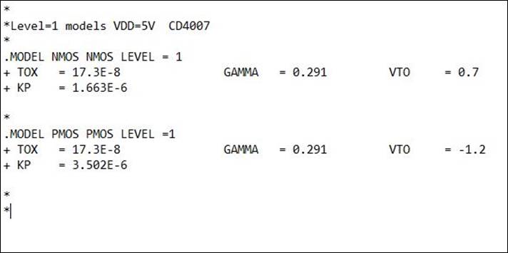
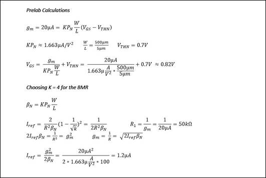
The pre-lab work is a basic BMR design. The model we are using to
calculate this design was developed in laboratory 8 and is displayed below to
the left. The hand calculations for the BMR design are displayed below to the
right.
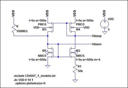
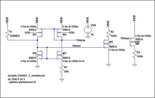
The circuit schematic is displayed to the left below. This is the same
schematic that will be utilized in the laboratory experimental procedures. The
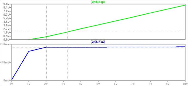
waveform resulting from sweeping VDD from 0V to 10V is displayed to the right.
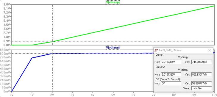
As predicted in the lab instructions, Vbiasn
stabilizes after VDD hits a minimum value of approximately 2V. Vbiasp also behaves as predicted, following VDD after
reaching the same approximate value. .
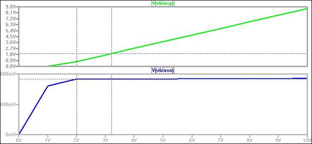
The simulated value of Iref is displayed
below. The simulated value approximates 1.0µA for the VDD sweep from 0V to 10V.
Experiment
1
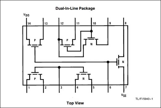
In this lab you may need to use two, or more, CD4007 chips from the same production
lot (see date code on the top of chip) to ensure using a BMR to bias a current
mirror is possible. If the CD4007 chips are not from the same production lot
they will not "match" so current mirrors will not be possible.
- Build your BMR design and
characterize it as you did in the pre-lab
- You expect the BMR to become
unstable if there is a large capacitance across the resistor, such as a
scope probe (important), so care must be exercised
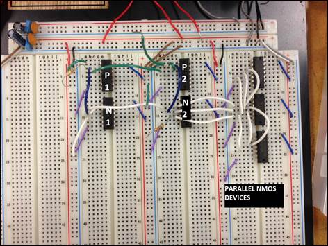
The initial wiring of the BMR proved to be challenging due to the
layout of the CD4007, as seen below. To try to minimize the error in the
circuit, the best design practice requires keeping the number of chips to a
minimum. However, the gates of the device are tied together in a manner that
made wiring confusing. Specifically, attempting to build the BMR resulted in
the gates of the two PMOS devices tied to the gates of one of the NMOS devices.
To simplify the experiment, up to eight chips were included, with one chip used
per device for the basic BMR structure. Thus, the BMR was designed using four
chips, the current mirrors added three more in parallel, and an additional chip
was used for finishing the cascode structure. The BMR
circuit design is displayed below to the right.
The table below shows the values for Vbiasn
and Vbiasp as VDD is swept from 0V to 10V. The values
closely parallel the simulated values.
|
VDD (V) |
Vbiasn (V) |
Vbiasp (V) |
|
0 |
0.00 |
0.00 |
|
1 |
0.877 |
0.331 |
|
2 |
1.08 |
0.579 |
|
3 |
1.13 |
1.56 |
|
4 |
1.17 |
2.55 |
|
5 |
1.19 |
3.54 |
|
6 |
1.22 |
4.54 |
|
7 |
1.24 |
5.53 |
|
8 |
1.25 |
6.53 |
|
9 |
1.27 |
7.52 |
|
10 |
1.29 |
8.52 |
The most noticeable difference between the simulations and
experimental values is the magnitude of Vbiasn. The
simulation results approximate 880mv versus an experimental magnitude near
1.3V. This is higher than expected, but could be attributed to errors in the
CD4007 model or experimental errors, including the use of so many chips.
However, the experimental waveform does model the simulated behavior, including
the estimated minimum VDD where Vbiasp follows VDD
and Vbiasn levels out.
Experiment 2
- Use your BMR to bias, and thus
create, a:
- NMOS current mirror
- PMOS current mirror
- Measure how the current varies
through each current mirror as the voltage across the mirror changes.
- Of course the current in the
NMOS (PMOS) current mirror goes to zero as the voltage on the drain of
the output device moves towards ground (VDD)
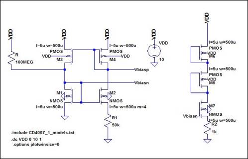
Adding the NMOS and PMOS current mirrors to the BMR proved to be
much simpler than the initial wiring. The circuit displayed to the left
includes the current mirrors with 100kΩ sampling resistors attached to
each device. These resistors are used with a multi-meter to measure the
voltages as VDD is swept and then basic circuit analysis is used via Ohm's Law
to calculate the drain current, ID, in each device. These values are
included with corresponding I-V curves further below. The simulation waveform
displayed to the right directly below illustrates the biasing remains constant
with the additional devices added to the circuit.
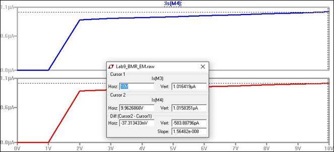
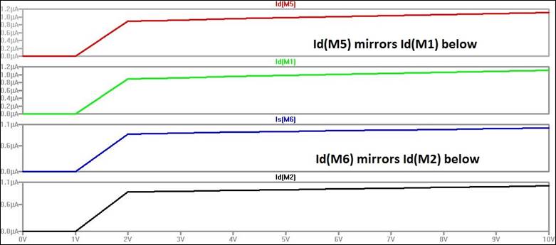
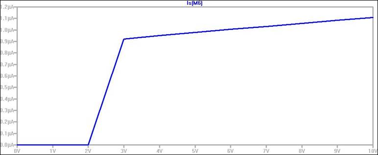
The waveform below displays the simulated values for the drain
currents, ID5 and ID6 , through
devices M5 and M6 in the schematic above. M5 is biased via Vbiasn
and M6 is biased via Vbiasp. Below ID5 is
the waveform for the current M5 is mirroring, ID1
, and below ID6 is the waveform for the current M6 is
mirroring, ID2 . Notice the
simulated currents are identical.
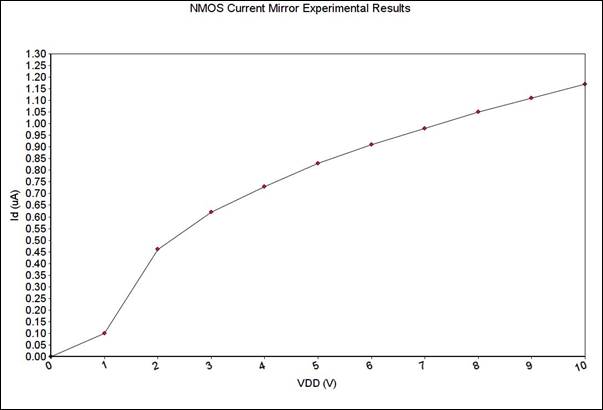
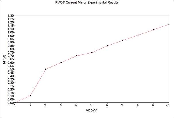
The experimental values for each current mirror are included in
the table below.
|
VDD (V) |
Id (uA) NMOS Mirror |
Id (uA) PMOS Mirror |
|
0 |
0.00 |
0.00 |
|
1 |
0.10 |
0.11 |
|
2 |
0.46 |
0.54 |
|
3 |
0.62 |
0.63 |
|
4 |
0.73 |
0.72 |
|
5 |
0.83 |
0.75 |
|
6 |
0.91 |
0.85 |
|
7 |
0.98 |
0.93 |
|
8 |
1.05 |
1.01 |
|
9 |
1.11 |
1.09 |
|
10 |
1.17 |
1.17 |
The data plotted below has characteristics similar to the
simulated waveforms, but does not model it exactly. This could be due to the
CD4007 model used in the simulations or possibly experimental errors. The
experimental plot shows the current requires a higher voltage before it begins
to flatten out.
Experiment 3
- Using these current mirrors
drive two gate-drain connected transistors
- For the first experiment use
the NMOS current mirror to drive two PMOS gate-drain connected
devices.
- Use the voltages on the
gate-drain connection of the two devices to bias a cascode
current mirror (characterize this mirror as before)
- For the second experiment
switch, that is, use the PMOS current mirror to drive two NMOS gate-drain
connected devices.
- Again, use these two voltages
to bias an NMOS cascode current mirror then
characterize.
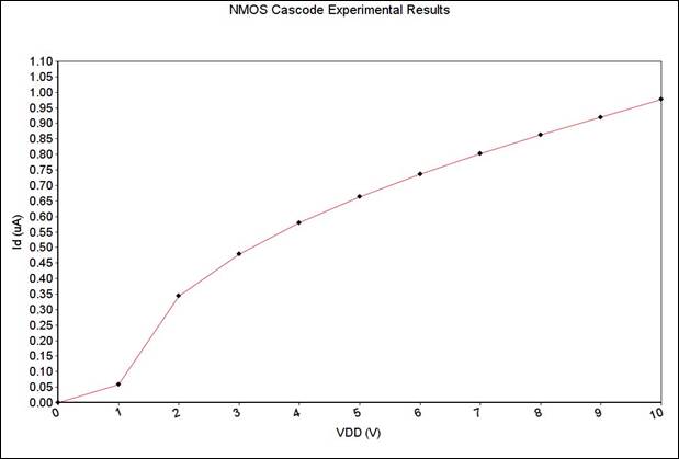
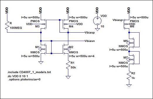
NMOS
Current Mirror with Two PMOS Gate-Drain Connected Devices
The
circuit for this experiment is displayed below to the left with the resulting
simulation waveform displayed to the right. The experiment used a 1k sampling
resistor to determine the current through the cascode
in the same manner as performed for the current mirror experiment above.
The
experimentally determined values are given in the table below.
|
VDD (V) |
Id (uA) NMOS Cascode |
|
0 |
0.00 |
|
1 |
0.06 |
|
2 |
0.34 |
|
3 |
0.47 |
|
4 |
0.58 |
|
5 |
0.66 |
|
6 |
0.74 |
|
7 |
0.80 |
|
8 |
0.86 |
|
9 |
092 |
|
10 |
0.98 |
The
waveform below is similar, but not the same as the simulation model, suggesting
there is an error in the model used for the simulations or an experimental error
was made in the laboratory. Numerous attempts were made to parallel the
simulation results by retracing the experimental circuit and changing measuring
equipment, but the results remained consistent when measured again.
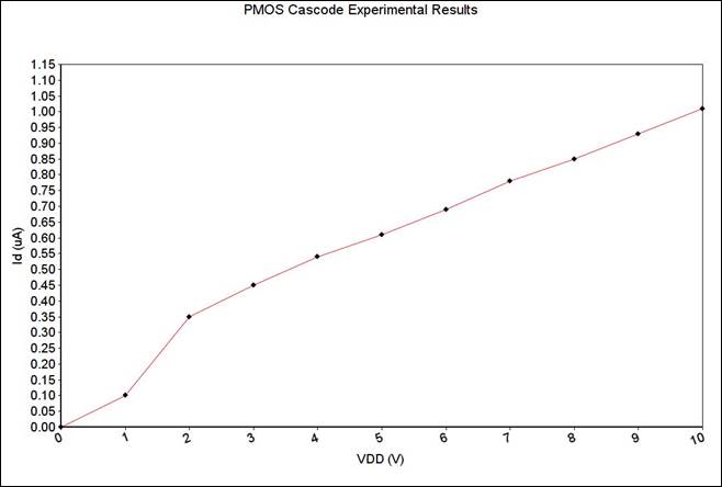
PMOS
Current Mirror with Two PMOS Gate-Drain Connected Devices
The
circuit for this experiment is displayed below to the left with the resulting
simulation waveform displayed to the right. The experiment used a 1k sampling
resistor to determine the current through the cascode.
The
experimentally determined values are given in the table below.
|
VDD (V) |
Id (uA) PMOS Cascode |
|
0 |
0.00 |
|
1 |
0.10 |
|
2 |
0.35 |
|
3 |
0.45 |
|
4 |
0.54 |
|
5 |
0.61 |
|
6 |
0.69 |
|
7 |
0.78 |
|
8 |
0.85 |
|
9 |
093 |
|
10 |
1.01 |
The PMOS waveform also
models the simulation results, but not exactly. The same error in either the
simulation model or the experimental procedures resulted in a data plot with
values that do not match the simulated values. Again, efforts to determine the source
of error yielded no solution.
Conclusion
Laboratory
experiment 9 presented numerous challenges regarding the design and
characterization of a Beta-Multiplier Reference (BMR) using the CD4007 CMOS
transistor array. The experience relating the CD4007 models developed in
laboratory eight with the design of the BMR in this experiment demonstrated the
complexity of building Spice models. The CD4007 model developed and used to
design the BMR still needs to be tested and refined, but the fundamental
strategy and method for continuing to develop SPICE models is the net result
achieved in this laboratory experiment.
Return to
Monahan Lab Report Directory