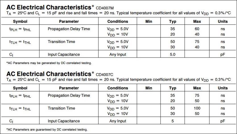
EE 420L Engineering Electronics II - Lab 8
4/13/16
Lab 8: Characterization of the CD4007 CMOS
transistor array
In this lab you will characterize the
transistors in the CD4007 and generate SPICE Level=1 models. Assume that the
MOSFETs will be used in the design of circuits powered by a single +5 V power
supply. In other words, don't characterize the devices at higher than +5 V
voltages or lower than ground potential.
- Experimentally
generate, for the NMOS device, plots of:
1.
ID v. VGS (0 < VGS < 3 V) with VDS = 3
V
2.
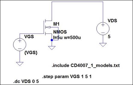
ID v. VDS (0 < VDS < 5 V) for VGS varying
from 1 to 5 V in 1 V steps, and
3.
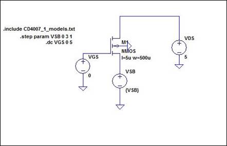
ID v. VGS (0 < VGS < 5 V) with VDS = 5 V
for VSB varying from 0 to 3 V in 1 V steps.
- Note
that for this last one, if VSS (NMOS body) is ground (again, the
Body, VB, is grounded) then the source voltage will be varied from 0 to 3
V in 1 V steps to realize VSB ( = VS - VB = VS)
varying from 0 to 3 V in 1 V steps. At the same time VGS will be varied
from 0 to 3 V (when VS = 0), 1 to 4 V (when VS = 1 V), 2 to 5 V (when VS =
2 V), and 3 to 5 V (when VS = 3 V). In other words, as VS is
increased by 1 V the VGS has to shift up by 1 V as well.
- Assuming
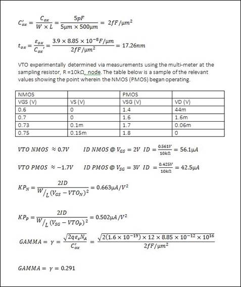
that the length of the NMOS is 5 um and its width is 500 um calculate
the oxide thickness if Cox (= C'ox*W*L) = 5 pF.
- From
this measured data create a Level = 1 MOSFET model with (only) parameters:
VTO, GAMMA, KP, LAMBDA, and TOX.
- Compare
the experimentally measured data above (the 3 plots) to LTspice-generated data (again, 3 plots) and adjust
your model accordingly to get better matching.
- Repeat
the above steps for the PMOS device where VDS, VGS, and VSB are replaced
with VSD, VSG, and VBS respectively.
Experiment
1:
Calculated
Values for the CD4007 Level = 1 model. The initially calculated values resulted
in the following values. These values resulted in simulation waveforms that
closely match the experimental waveforms.
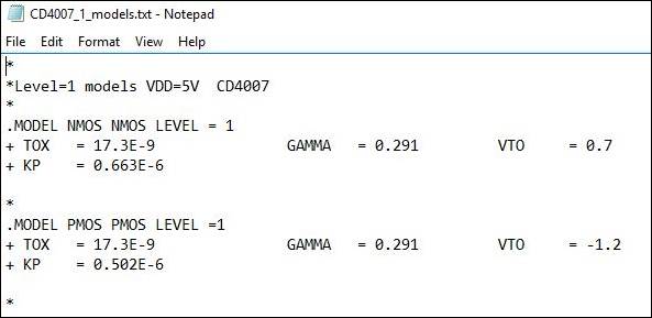
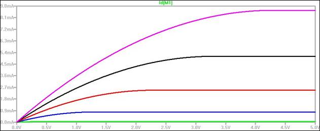
The
CD4007 model above
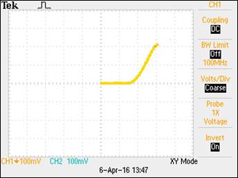
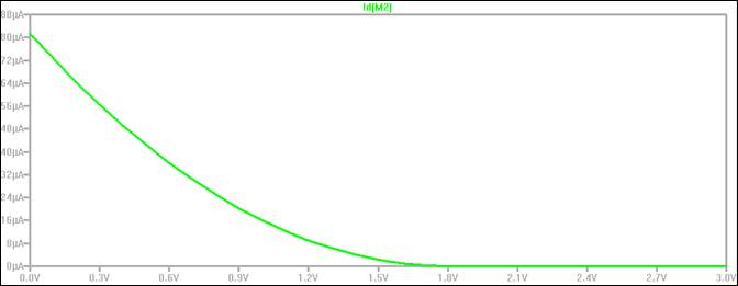
NMOS
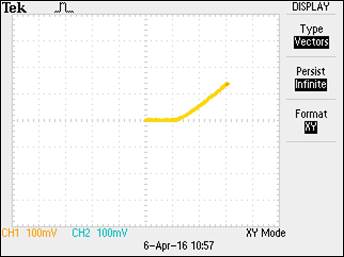
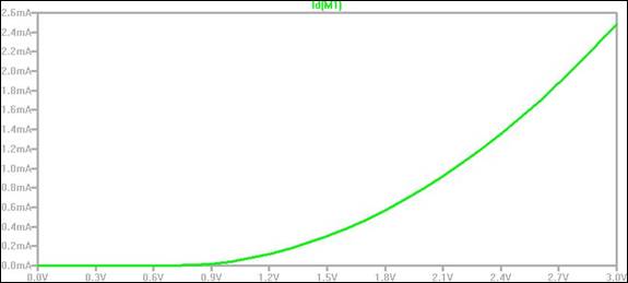
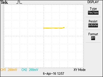
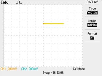
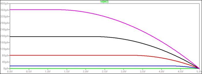
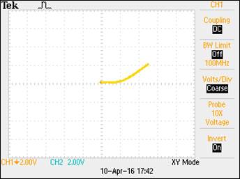
ID v. VGS (0 < VGS < 3 V) with VDS = 3 V. The simulated
waveform using the CD4007_models.txt file is seen below. This is closely
matched to the experimental waveforms seen below.
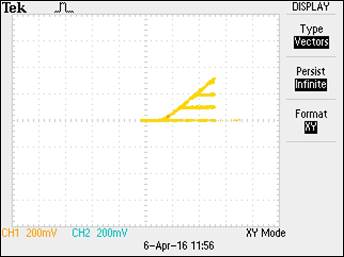
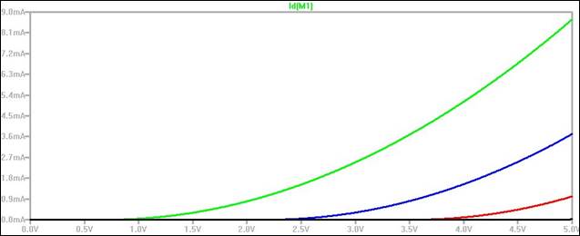
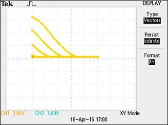
ID v. VDS (0 < VDS < 5 V) for VGS varying
from 1 to 5 V in 1 V steps.
ID v. VGS (0 < VGS
< 5 V) with VDS = 5 V for VSB varying from 0 to 3 V in 1 V steps
Left to Right: VSB =0V,
1V, 2V and 3V seen below. To obtain the potential between the source and bulk,
a voltage divider was used between VDD and the sampling resistor. This allowed
for a simple and efficient method of creating the necessary potential using 1kΩ,
2 kΩ, 3 kΩ and 4 kΩ resistors.
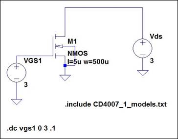
These
are the schematics for the NMOS simulations for Experiment 1, parts 1, 2 and 3,
respectively.
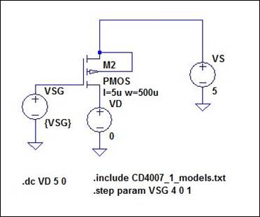
PMOS
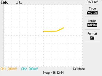
The
PMOS presented a challenge to measure properly. The 10kΩ sampling
resistor was too large and needed to be replaced by a 1kΩ resistor to
obtain the proper waveform.
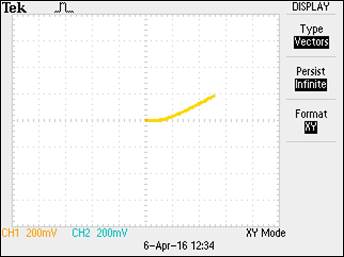
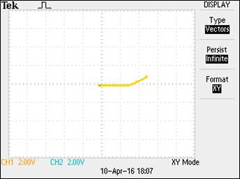
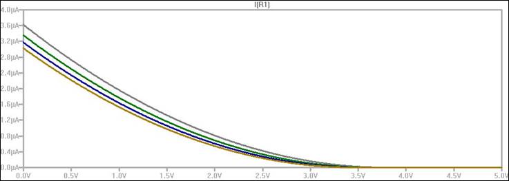
ID v. VSG (0 < VSG < 3 V) with VSD = 3 V. Notice the
oscilloscope waveform is inverted, thus the waveforms are the same.
ID v. VSD (0 < VSD < 5 V) for VSG varying from 1 to 5 V in 1
V steps
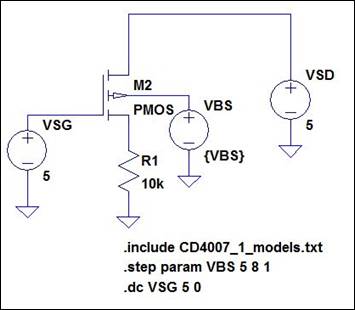
ID v. VSG (0 < VSG
< 5 V) with VSD = 5 V for VSB varying from 0 to 3 V in 1 V steps
Left to Right: VBS =0V,
1V, 2V and 3V seen below. The waveforms for 2V and 3V were scaled larger to
make the curve more noticeable.
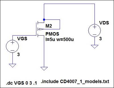
These
are the schematics for the PMOS simulations for 1, 2 and 3, respectively.
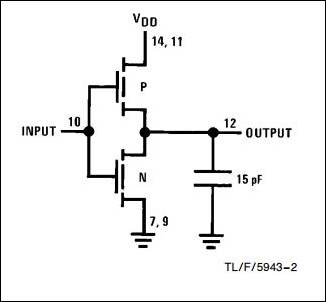
Experiment 2:
- Experimentally,
similar to what is seen on the datasheet (AC test circuits seen on page 3
of the datasheet), measure the delay of an inverter using these devices
(remember the loading of the scope probe is around 15 pF and there is
other stray capacitance, say another 10 pF).
- Using
your model simulate the delay of the inverter and compare to measured
results. Adjust your SPICE model to get better matching between the
experimental data and the measured data.
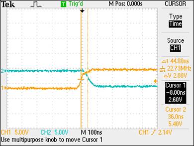
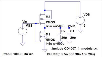
The AC circuit displayed
to the left below was used to measure the inverter delay.
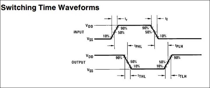
The inverter delay waveform
is pictured below. The 44.00ns delay is within the range of values given on the
datasheet.
The initial Spice
simulation using the CD4007 model resulted in the following waveform.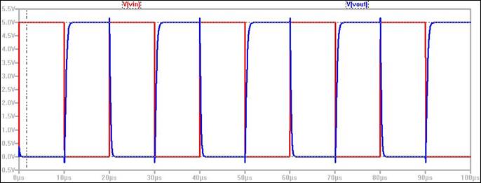
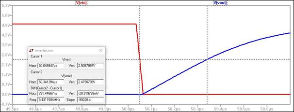
There is obviously a
small capacitance issue on the output. I increased the distance of TOX by a factor of 10 to see if reducing the
internal capacitance of the NMOS and PMOS would change the output and result in
a better inverted output. The results of the changed CD4007 model and the
schematic are displayed below. The drawback is the delay time is not comparable
to the delay time measured experimentally. The experimental value was 44.0ns
versus 291.5ns in the simulation.
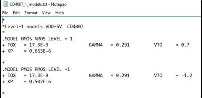
The updated CD4007 Model
is included below.
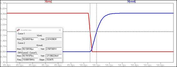
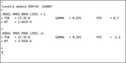
However, this delay
issue is unsatisfactory. I next increased the values of KP for both devices.
The results of this final adjustment to the model resulted in a satisfactory
output that is comparable to the experimentally determined values. The delay is
now an acceptable 50.8ns.
Conclusion
The
experiments conducted in Laboratory 8 demonstrated the procedure for
determining the characteristics of a CMOS transistor and utilizing these
characteristics to create a Level = 1 MOSFET Spice model. The experiments also
presented the opportunity to obtain the I-V characteristics of the CD4007
transistor and to practically apply the data gathered to model the CD4007 and
analyze the behavior of the device in simulations.
Return to
Monahan Lab Report Directory
Return
to EE 420L Spring 2016 Student Directory