EE 420L Engineering Electronics II - Lab 7
4/6/16
Design
of an audio amplifier
This lab will
again utilize the ZVN3306A and ZVP3306A MOSFETs.
Design an audio amplifier (frequency range from roughly 100 Hz to 20
kHz) assuming that you can use as many resistors, ZVN3306A transistors, and
ZVP3306A transistors as you need along with only one 10 uF
capacitor and one 100 uF capacitor. Assume that the
supply voltage is 10 V, the input is an audio signal from an MP3 player (and so
your amplifier should have at least a few kiloohms
input resistance), and the output of your design is connected to an 8-ohm
speaker (so, ideally, the output resistance of your amplifier is less than 1
ohm).
Your lab report should detail your thoughts on the design of the
amplifier including hand-calculations. A good place to start is with the
push-pull amplifier characterized in lab 6. Simulate your design. Document the
results in your lab report.
Experiment
The first part of the experiment
involved contemplating a design based upon the push-pull amplifier included in
the Laboratory 7 instructions. The choice is logical due to the high gain that
results from the basic push-pull topology illustrated in Laboratory 6,
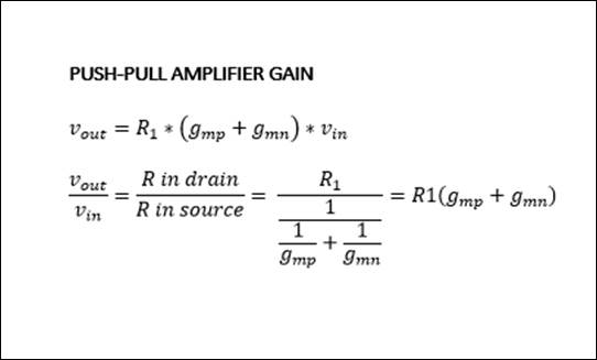
Experiment 4. The basic topology and gain are displayed below as a review.
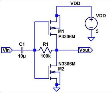
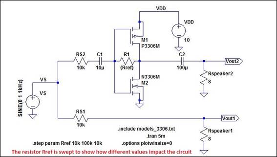
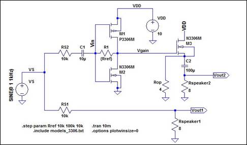
The schematic presented in the
Laboratory 7 instructions is displayed below. The resistor R1 is proportional
to the gain of the circuit. Laboratory 6 experimentation led to experimental
values of gmn equal to 19.0mA/V and gmp equal to 13.3mA/V.
This presents a constant in our gain. Sweeping R1 allows analysis of the
circuit operation for different gains.
Ideally, this allows a design that will maximize our gain and minimize
our power consumption. The speaker used in the experiment is only 2W and the
transistor has a power dissipation around 600mW, so
the power cannot be too high.
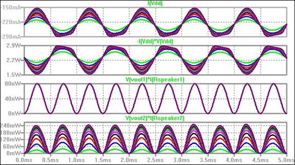
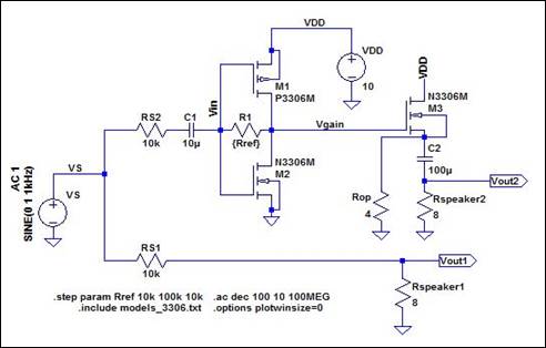
The waveform displayed above to the
right shows the plots for all the different values of R1 from 10kΩ to
100kΩ. Top to bottom, these include the current in the circuit centered
at 220mA with a 70mA swing, the average power centered at 2.2W with a 0.7W
swing, the power through the speaker that does not receive amplification and
the power through the speaker receiving amplification. Note the difference in
power in speaker 2 approximately 3 times the power in speaker one. Looking at
the waveforms, it is easy to see there is a point where the increasing
resistance starts to adversely impact the circuit with clipping. This will be
dealt with after the next design consideration.
The issue with this basic design is
that despite the ability to set the gain by simply changing the value of R1,
the amplifier needs to have an output impedance lower
than the speaker impedance of 8Ω. The goal is a high input impedance to
allow amplification of the voltage and a low output impedance to drive the
current up. To lower output impedance, a source-follower was added to the
output of the initial push-pull stage. The source-follower has a unity gain and
low-output impedance, thus the benefit of the push-pull gain is preserved with
the additional benefit of a smaller output impedance.
The circuit below is the new circuit with the source follower added and an
additional 8Ω resistor added to further reduce output resistance. The
waveform to the right is the initial gain with R1 again being swept. Clearly,
using too large of a resistor has a negative impact on the gain. To determine a
gain that works, the steps were singled out in the simulation until a suitable
resistance was determined.
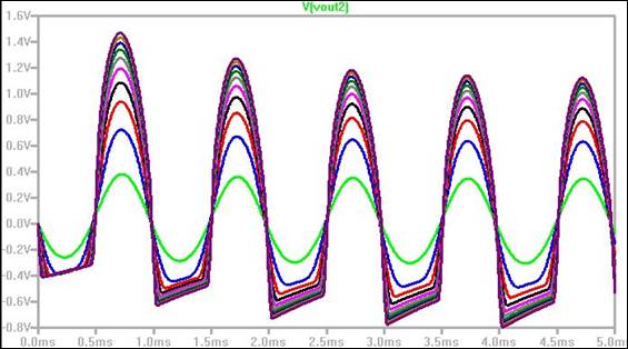
The top waveform below displays the
output versus the input at R1 = 30kΩ. There is clearly clipping occurring
at the output. The remaining three waveforms are, top to bottom, the current,
power dissipation and output versus input with R1 = 20kΩ. Notice the
difference in power and current at the output. Adding the source-follower stage
to the initial push-pull stage resulted in a 200mA increase with a 220mA swing.
The power is now centered at 4.2W with a 2.2W swing. This led to the decision
to use a 20kΩ resistor for R1. This will provide a theoretical gain of Av =
20kΩ*(19mA/v+13.3mA/V) = 3230V/V.
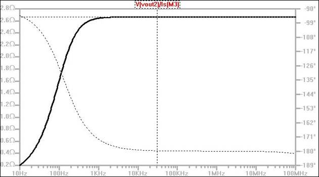
As predicted, the source follower
also resulted in a reduction in output resistance as seen in the waveform on
the bottom. The output impedance is approximately 2.67Ω, a result of R2
in parallel with the 8Ω speaker load. This is simply (4*8)/12 or
approximately 2.67Ω as displayed.
The result of the simulation is an
amplifier that provides enough power and current to drive the MP3 player.
Build and test your design. Document the
performance of the design including power dissipation, output swing, input resistance,
output resistance.
This
is the initial circuit with a 200kΩ potentiometer as R1. The initial plan
was to sweep the pot until the best sound and gain was heard
and ultimately treat the pot as a volume control. However, given my
limited experience with amplifier design this may not have been the best
approach. This resulted in more confusion than the effort was worth and was
quickly replaced by a 20kΩ resistor. The inclusion in the report is
simply to show the initial approach and verify there is more failure than
success in the laboratory.
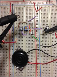
Building
and testing the design presented a challenge. The initial design resulted in
some amplification and a high pitched sound coming from the speaker with a
sinusoidal input of 1VPP@1kHz. However, the amplification was small and the
current was only 150mA. Varying the frequency from 100Hz to 20kHz
did not result in any sound at all. To attempt to increase the gain in the
push-pull stage, a second PMOS and NMOS were added in parallel to the initial
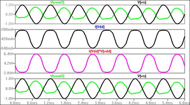
devices in the schematic above. A second
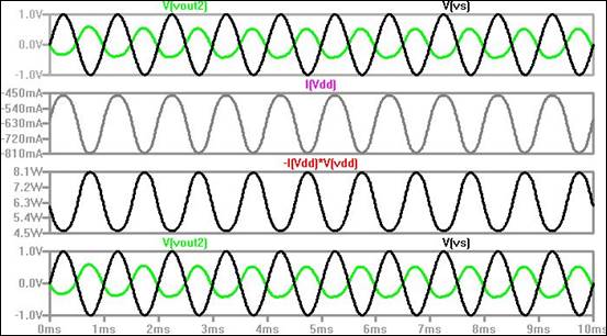
NMOS was also added into the source follower to drive the current up. The
simulations below show the results. Note the large increase in current I(Vdd). The power also increased
considerably.
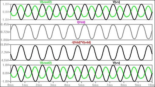
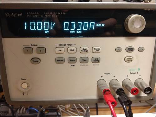
When this
stage was added the current in the power supply jumped up to 338mA and the
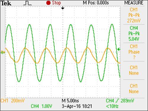
sound was distorted. The waveform to the right below displays Channel 4 with a
voltage gain of approximately 18. Testing the frequency at 100Hz and 20kHz resulted in some noise, but not a clear sound as with
1kHz. The transistors were also noticeably warmer.
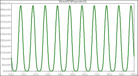
To
lower the current gain, the second parallel NMOS was removed from the source
follower stage and the circuit was simulated again. The results are displayed
below. Note the current and power decreased. The maximum power through the
speaker is approximately 420mW as displayed in the waveform to the right. The
power dissipation for the NMOS is rated at approximately 625mW at room
temperature, but this transistor is definitely hotter than room temperature.
Theoretically, the power is within the margins, but practically the power is
too high.
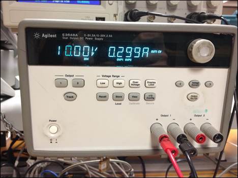
After removing the parallel NMOS
from the source follower, the current dropped down to 299mA. This gives us an average
power of approximately 2.99W. This is a little higher than desired, but for the
laboratory experiment, this is satisfactory. The resulting waveform below shows
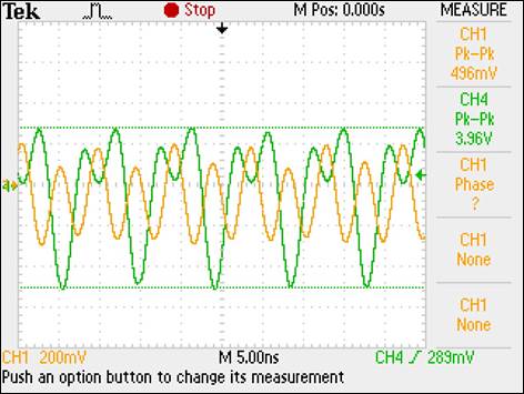
a voltage gain of approximately 8V/V where Av = 3.96V/496mV. The
sound coming from the speaker at 1kHz was clear and
high pitched, superior to the distorted sound prior to removing the second
parallel NMOS. The sound at 100Hz was cleaner, but still had crackling and some
distortion. At 20kHz there was a consistent static
sound.
Conclusion
The experiment conducted in
laboratory seven provided the opportunity to design an audio amplifier and gain
practical experience with the trade-offs involved in analog design.
Specifically, learning how to utilize different topologies to take advantage of
the inherent characteristics of each design requires study and experimentation.
This laboratory offered an excellent chance to learn about manipulating input
and output impedances to achieve a desired effect. Learning to create unique
designs using different amplifier topologies in varying stages and
comprehending how each decision impacts the overall circuit is a skill acquired
via practical application.
Return to
Monahan Lab Report Directory
Return to EE420L
Spring 2016 Student Directory