EE 420L Engineering Electronics II - Lab 6
3/30/16
Lab 6: Single-stage transistor amplifiers
Experiment
1
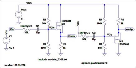
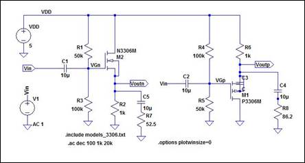
Below are schematics for NMOS and PMOS source followers amplifiers (also known as common-drain
amplifiers).
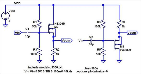
In your lab report discuss the operation of these circuits.
The common drain
amplifier displayed above is also known as the source follower. The gate serves
as the input terminal and the source serves as the output terminal with the
drain common to both the input and the output, thus the amplifier is known as
the "common drain". The
benefit of using a source follower is the amplifier has a voltage gain of one
with a current gain. An amplifier with a voltage input ideally has both an infinite input impedance resulting in zero input current
and a low output impedance. To achieve a current gain, the resistor R2
at node VOUT creates a potential, VSB , between the source and body if the body is
tied to ground. VSB results in body effect and a resultant increase
in VTH that consequently causes a current to flow, thus achieving a
current gain.
The voltage divider in
front of the gate is used to set the biasing and the resistor in the source is
used to determine the gate to source voltage so the device is operating in the
saturation region. A capacitor is used with the input for AC coupling so the
biasing is not impacted at the gate. The output is measured at the source.
Simulate the operation of these amplifiers. Hand calculate, and
then verify your hand calculations with experimentation and simulations,
the gains and the input and output resistances ensuring that your
test signals are at a high enough frequency that the caps have negligible impedance
but not so high that the gain is dropping off. If you build this circuit using
electrolytic capacitors, assuming the input AC signal swings around
ground, put the "+" terminal of the cap on the gate of the MOSFET.
Please indicate, in your lab report, that you understand why the capacitor is
connected this way.
Regarding electrolytic capacitors:
The circuits in the
laboratory experiments were all built utilizing electrolytic capacitors.
Electrolytic capacitors are polarized and use a chemical reaction between the
anode and cathode to form an insulating layer. If the electrolytic capacitor is
reverse-biased, the chemical reaction is reversed and eats away the insulating
layer, effectively creating a short between the terminals. The result is any
significant voltage across the capacitor can cause the capacitor to overheat
and explode. Thus, the more positive voltage in a circuit receives the positive
terminal of the capacitor.
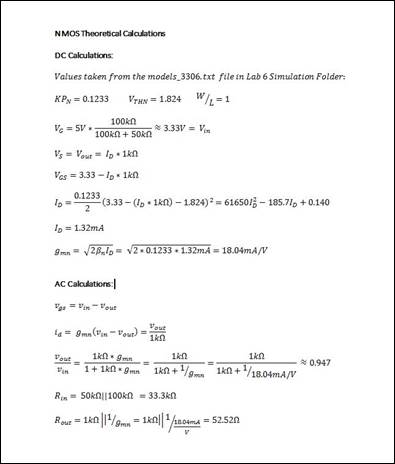
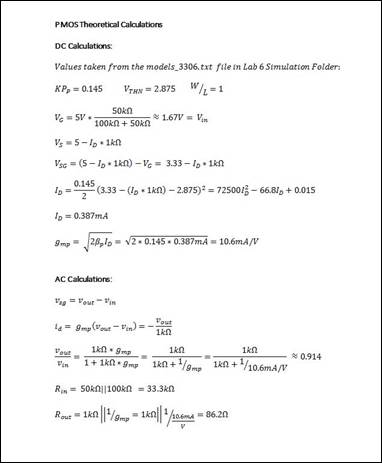
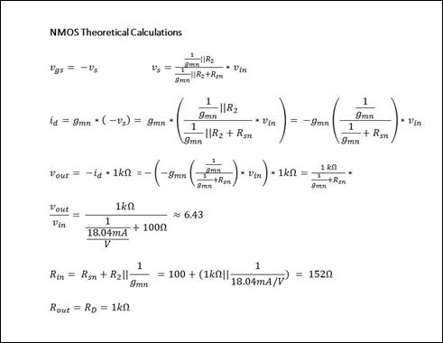
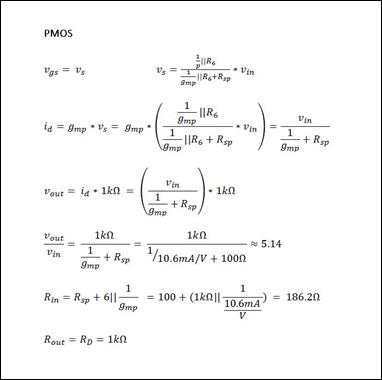
Theoretical Results
The images below contain
the AC and DC calculations for the Source Follower.
Simulation Results
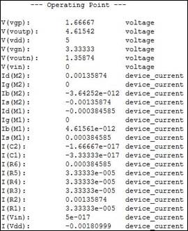
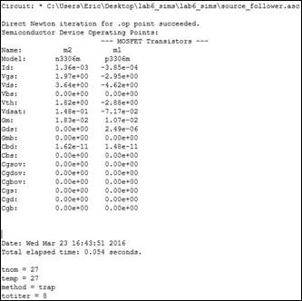
The simulations for the source follower are
included in the images below. The image to the left displays the DC voltages
with values similar to the theoretical values calculated above. The image to
the right displays similar values for the transconductance,
gm, for each device. The Spice Error Log
will be excluded in the remaining experiments, as the gm
values below will hold for the remaining experiments. These are 18.3mA/V for
the NMOS and 10.7mA/V for the PMOS.
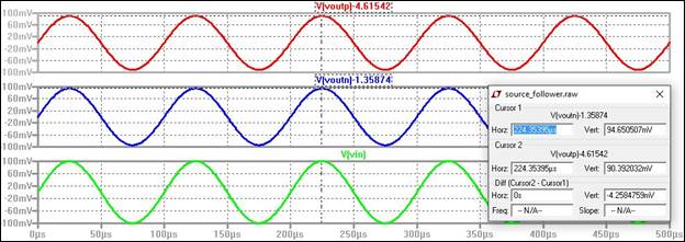
The transient simulation
vales for gain are similar to the theoretical calculations performed above. The
NMOS displays a gain of 0.946 and the PMOS displays a gain of 0.904 on a 100mV
input.
In your lab report discuss, in your own words, how to measure
the input resistance.
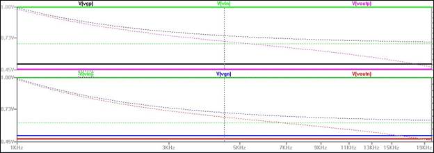
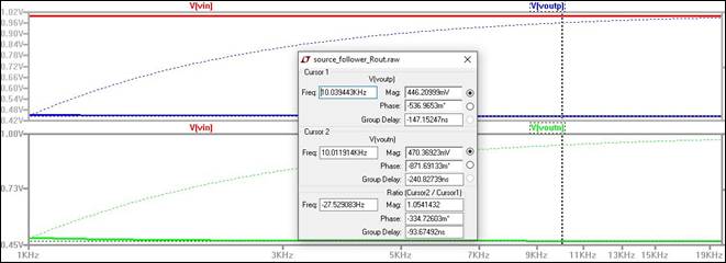
To measure the input
resistance in the simulation and in the laboratory experiment, a resistor
equivalent to the calculated value of the input resistance, 33kΩ, is placed in series to the input resistance. This forms a voltage
divider that will result in half the input voltage and consequently, half the
output voltage. The circuit and simulation are displayed below. The top
waveform displays the PMOS circuit with Vin ,
Vgp after the voltage divider and Vout . The values clearly display the voltage
after the divider at approximately one half the input
and the output voltage also now one-half. The same results apply to the lower
waveform for the NMOS. The slight
difference in the output being less than half can be explained by the
difference in calculated gain being slightly less than one for both the NMOS
and the PMOS.
Again, in your lab report discuss how to measure the
output resistance.
In a similar manner, to measure the output resistance we can use
the theoretical values, 52.5Ω for the NMOS and 86.2Ω for the PMOS,
calculated earlier. A coupling capacitor
in series with the resistor can be placed in parallel in the respective
circuits with the 1kΩ resistor connected to the source. This is the same
concept applied above for the input resistance. The output voltage is now
connected to a voltage divider that will result in half the output voltage.
This is useful in practical applications in the laboratory due to the basic
concepts of voltage division. If the output voltage is not halved for either
measurement of Rin or Rout, but
the other values are measured, the real input or output resistance can be
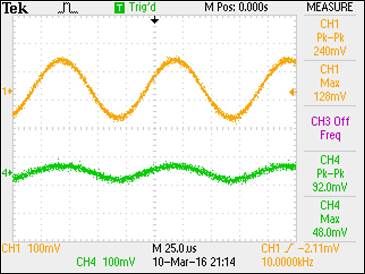
solved for by simple algebra. The circuit used to measure output resistance and
the resulting waveforms are displayed below. The top waveform displays the PMOS
output at approximately one half the input and the lower waveform displays the
same for the NMOS circuit, thus verifying the theoretical values.
Experimental
Results
All
experiments performed with a 10kHz sinusoidal input.
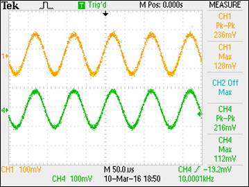
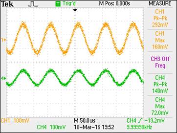
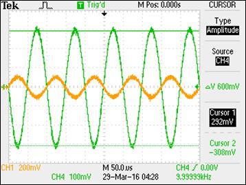
GAIN: NMOS displayed to the left. PMOS displayed to the right. The output on Channel 4 is approximately
0.915 for the NMOS and 0.867 for the PMOS. This is similar to the theoretical
and simulated values.
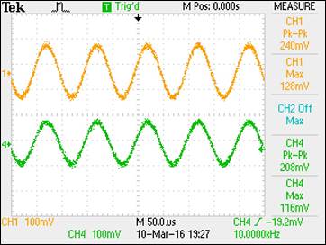
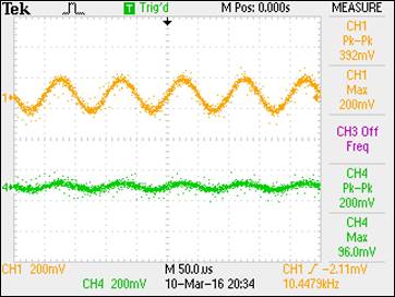
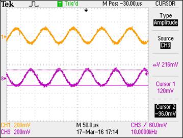
Rin : NMOS displayed to the left. PMOS displayed to the right. The NMOS
output on Channel 4 is approximately one half the input
displayed on Channel 1 with the same result displayed for the PMOS. This was achieved
using the procedure outlined and simulated above.
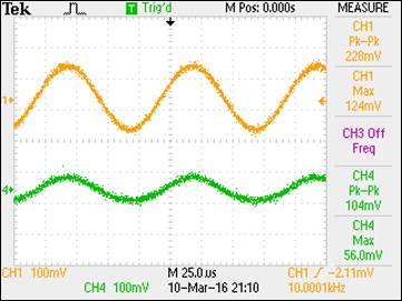
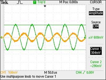
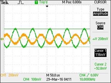
Rout: NMOS displayed to the left. PMOS displayed to the right. The NMOS
displayed a value slightly less than one half on the output, but this is
consistent with the measured gain. Multiplying the output by
2 results in 208mV. Dividing this by the input, 228mV, results in a gain of 0.912. This is consistent with the
measured values achieved earlier. The same concept applies to the PMOS,
however, this technique results in a gain of only 0.777 for the PMOS. This
implies the output resistance of the device is not precisely as calculated. The
measurement of transconductance, gmp, necessary to recalculate Rout,
was performed by measuring the voltages across the 1kΩ resistor connected
to the PMOS source and solving for the current. This resulted in a transconductance, gmp,
of approximately 13.3mA/V versus 10.6mA/V theoretical. The resulting
recalculation showed a Rin of
approximately 70Ω.
Experiment 1 Table of Values
|
NMOS |
Theoretical |
Simulation |
Experimental |
|
Gain |
0.947 |
0.946 |
0.915 |
|
Rin (Ω) |
33k |
33k |
33k |
|
Rout (Ω) |
52.5 |
52.5 |
52.5 |
|
PMOS |
|
|
|
|
Gain |
0.914 |
0.904 |
0.867 |
|
Rin (Ω) |
33k |
33k |
33k |
|
Rout (Ω) |
86.2 |
86.2 |
70 |
Experiment
2
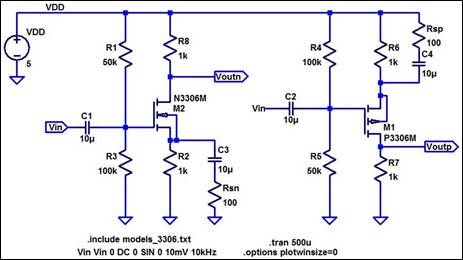
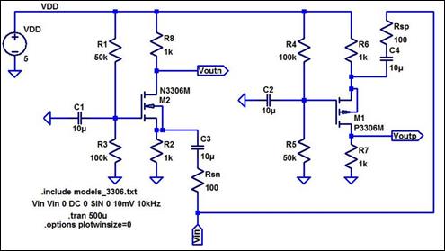
Below are two common-source amplifiers.
Discuss the operation of these amplifiers in your lab
report including both DC and AC operation. Hand
calculate the gains and the input/output resistances. How does the
source resistance, Rsn or Rsp,
influence the gain.
The common-source(CS) amplifier has the input at the gate and the
output at the drain of the device, thus the input and output have the source in
common. The voltage divider at the gate and the resistors in the drain and
source provide biasing and are set to keep the devices in the saturation
region. The capacitors are used for AC coupling, as in the source-follower.
Unlike the source-follower, the CS is utilized when a larger gain is
desired.
The gain is manipulated
via the two resistors, Rsn and Rsp. These resistor values can be increased or
decreased to modulate the current and thus the voltage at the output. Increasing the value of Rsn or
Rsp results in a decreasing gain, while
decreasing the value results in an increasing gain. This is verified via
the theoretical calculations, where Rsn
and Rsp are shown to be inversely
proportional to gain.
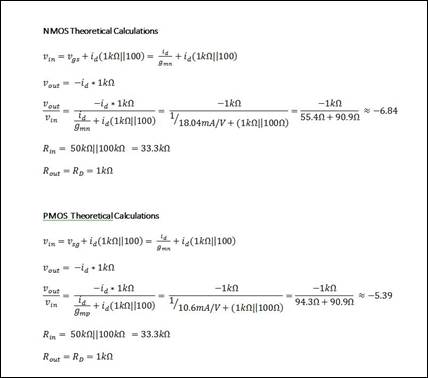
Theoretical Results
The calculations for the
given CS amplifiers are displayed below. These include the gain, Rin, and Rout.
Again compare your hand calculations to simulation and
experimental results.
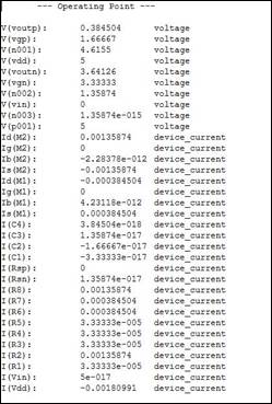
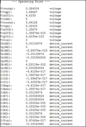
Simulation Results
Notice the biasing is
identical to the first circuit. The current in each device is the same as are
the gate voltages. The same techniques employed to simulate Rin
and Rout in Experiment 1 will be repeated in the simulations and
experiments in Experiment 2.
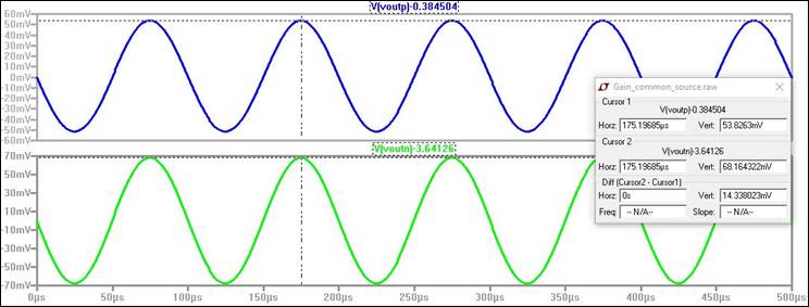
The gain for the two CS
amplifiers is similar to the theoretical calculated gain. Using a 10mV input
resulted in a gain of 6.81 for the NMOS and 5.38 for the PMOS.
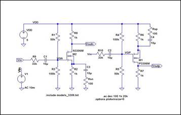
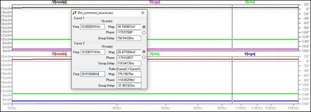
Simulating Rin results in the circuit and waveform
displayed below. Note the voltage output
is approximately one-half the output in the gain waveform above for the same
10mV input. The top waveform is for the PMOS and displays Vin
at 10mV, Vgp at 5mV and Vout at 26.47mV, approximately one-half the
output displayed above. The NMOS shows similar values with a gain of
approximately one-half, as well.
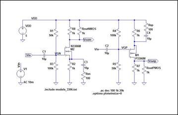
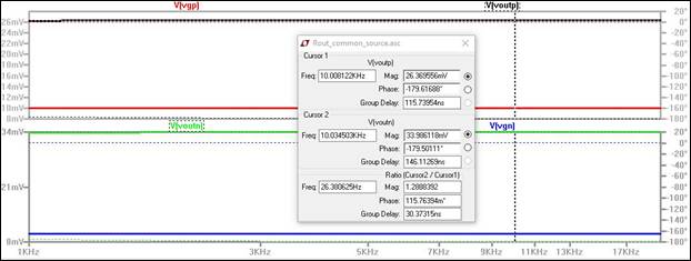
Simulating Rout
results in the circuit and waveform displayed below. The top waveform again
shows the gain is one-half the initial gain prior to adding the 1kΩ
resistor at Vout. The NMOS in the lower
waveform below displays a 33.9mV output on a 10mV input versus 68.2mV without
the voltage divider. The PMOS in the upper waveform displays a 26.3mV output
versus a 53.8mV output without the divider. Again, this method verifies the
theoretical calculations.
Experimental Results
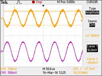
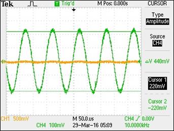
GAIN: NMOS input displayed to the left. NMOS output
displayed to the right. The resulting waveform was very thick due to
noise in the circuit. This resulted in seemingly inaccurate measurements,
however the noise in the waveforms caused the output to swing farther away from
the average than the oscilloscope could accurately display. The solution was to
use the cursors to try to measure the middle of the peak. This resulted in
values that were similar to our theoretical and simulation values. Most of the
experimental waveforms will be presented in this manner throughout the remainder
of this report. The NMOS input on Channel 1 displays 180mV pk-pk
and the output on Channel 3 displays 1.20V pk-pk.
This results in a gain of 6.7.
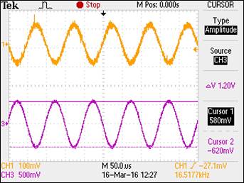
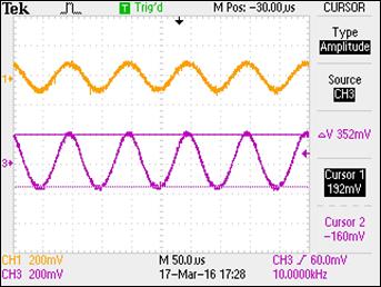
PMOS input displayed to the left. PMOS output displayed to the right.
Similar to the NMOS, the PMOS input on Channel 1 displays 184mV pk-pk and the output on Channel 3 displays 432mV pk-pk. This results in a gain of 2.35. This is not close to
the calculated or theoretical values. Troubleshooting failed to yield a gain
approximating theoretical or simulation values. The transconductance
was calculated experimentally by measuring the voltage at the drain and solving
for the current, however this yielded the same approximate value of 13.3mA/V as
calculated in Experiment 1. Other attempts to solve the issue included changing
the PMOS, rebuilding the circuit and retesting all elements within the circuit,
changing lab equipment and recalculating the gain. However, 2.35 was the best
gain achieved.
Rin : Rin is measured experimentally in the same manner as in the
simulation. The NMOS results below display the output at approximately one half
the initial gain prior to adding the 33kΩ
resistor. Channel 4 below displays the output at 600mV exactly one half the initial
gain of 1.2V, thus verifying the calculated input resistance matches the
experimental input resistance.
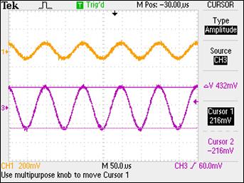
The results for the PMOS are displayed similarly. Notice the gain
at 208mV is approximately one-half the initial gain of 432mV.
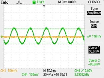
Rout: The NMOS waveform for Rout is
displayed to the left below. Note the output on Channel 4 is again one half the
initial gain of 1.2V achieved. Again, this verifies the theoretical value of 1kΩ
for Rout . The PMOS output waveform is
displayed to the right below. The addition of the voltage divider functioned as
expected and resulted in a gain equal to approximately one-half the initial
gain of 432mV.
Experiment 2 Table of Values
|
NMOS |
Theoretical |
Simulation |
Experimental |
|
Gain |
-6.84 |
-6.81 |
-6.7 |
|
Rin (Ω) |
33k |
33k |
33k |
|
Rout (Ω) |
1k |
1k |
1k |
|
PMOS |
|
|
|
|
Gain |
-5.39 |
-5.38 |
-2.35 |
|
Rin (Ω) |
33k |
33k |
33k |
|
Rout (Ω) |
1k |
1k |
1k |
Experiment
3
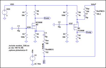
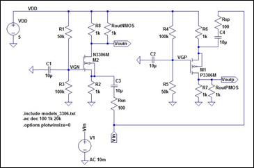
Below are two common-gate amplifiers.
Discuss the operation of
these amplifiers in your lab report including both DC and AC operation. Hand calculate the gains and the input/output resistances.
How does the source resistance, Rsn or Rsp, influence the gain.
The common gate (CG) has
the input on the source and the output on the drain, thus resulting in the gate
being common to both the input and the output. The CG amplifier has the
characteristics of low input impedance and high output impedance. The result is
a high voltage gain, but a low current and power gain. This circuit is DC
biased the same way as the source follower and the common-source amplifiers.
The source resistances, Rsn and Rsp ,
are still inversely proportional to the gain and thus cause the gain to increase
when they are decreased and cause the gain to decrease when they are increased.
This will be demonstrated in the calculations below.
Theoretical Results
The calculations for the
given CG amplifiers are displayed below. These include the gain, Rin, and Rout.
Again compare your hand calculations to simulation and
experimental results.
Simulation Results
Notice the biasing is
identical to the first two circuits. The current in each device is the same as
are the gate voltages. The same techniques employed to simulate Rin and Rout in Experiments 1 and 2
will be repeated in the simulations and experiments in Experiment 3.
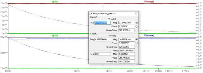
The gain for the two CG
amplifiers is similar to the theoretical calculated gain. Using a 10mV input resulted
in a gain of 6.21 for the NMOS and 4.76 for the PMOS.
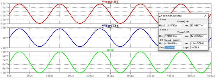
Simulating Rin results in the circuit and waveform
displayed below. Note the voltage output
is approximately one-half the output in the gain waveform above for the same
10mV input. The upper waveform displayed below shows the PMOS output at 24.1mV
versus 47.6mV in the gain waveform above. The lower waveform displayed below
shows the NMOS output at 31.0mV versus 62.1mV in the gain waveform. Again, this
verifies the input resistance approximately matches the theoretically
calculated value.
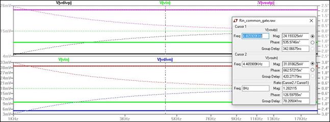
Simulating Rout
results in the circuit and waveform displayed below. The top waveform again
shows the gain is one-half the initial gain prior to adding the 1kΩ
resistor at Vout. The NMOS in the lower
waveform below displays a 30.8mV output on a 10mV input versus 62.1mV without
the voltage divider. The PMOS in the upper waveform displays a 24.1mV output
versus a 47.6mV output without the divider. Once again, the simulation verifies
the theoretical output resistance.
Experimental
Results
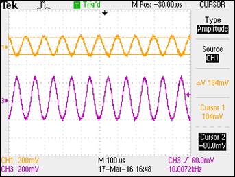
GAIN: NMOS input on Channel 1 displayed to the left. NMOS output on
Channel 2 displayed to the right. The gain is displayed to be 860mv/144mv, or
approximately 5.97.
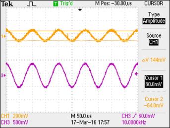
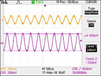
PMOS input on Channel 1 displayed to the left. PMOS output on
Channel 2 displayed to the right. The gain is displayed to be 352mv/168mv, or
approximately 2.09.
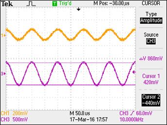
Rin: Rin is measured
experimentally in the same manner as in the simulation. The NMOS output waveform
to the right below displays the gain at approximately one-half the initial gain
after adding the 152Ω resistor to the input as in the simulation
schematic. The initial output displayed
above is 860mV versus 440mV displayed below. This confirms the input resistance
calculation is fairly accurate. The PMOS output waveform is displayed to the
left below. Again, after adding the 186Ω resistor to the input the output
is one-half the gain without the resistor. This confirms the theoretical
calculation for the output resistance.
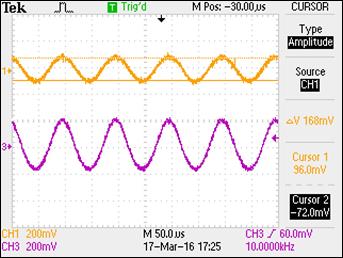
Rout: The NMOS output waveform is displayed to the
left below. The PMOS output waveform is displayed to the right below. The
addition of a 1kΩ resistor created a voltage divider and as expected,
both output waveforms are approximately one-half the initial output gain.
Experiment 3 Table of
Values
|
NMOS |
Theoretical |
Simulation |
Experimental |
|
Gain |
6.43 |
6.21 |
5.97 |
|
Rin (Ω) |
152 |
152 |
152 |
|
Rout (Ω) |
1k |
1k |
1k |
|
PMOS |
|
|
|
|
Gain |
5.14 |
4.76 |
2.09 |
|
Rin (Ω) |
186.2 |
186.2k |
186 |
|
Rout (Ω) |
1k |
1k |
1k |
Experiment
4
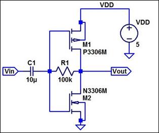
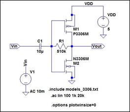
Below is a push-pull amplifier.
Discuss the operation of this amplifier in your lab report including
both DC and AC operation. Hand calculate the
gain of this amplifier. Do you expect this amplifier to be good at
sourcing/sinking current? Why or why not? What happens to the gain if the 100k
resistor is replaced with a 510k resistor? Why?
A push-pull amplifier is
designed to have an output that can drive a current in two directions through a
load. To implement a push-pull amplifier, a PMOS and an NMOS are used to source
current through the load and sink current from the load. These amplifiers are
used for low distortion, high efficiency and high output power. The circuit
uses the 5V DC source for biasing. The input and output are tied by the 100kΩ
resistor allowing the circuit to be self-biased with no DC current flow in the
transistors. The output is also limited by the rails. A positive input current
causes the gate of M1 to increase until it is cut off while the gate of M2 also
increases and turns on. If the input current is negative, the opposite
occurs. A positive AC input current
results in the gates of both devices increasing and shutting off M2. The
circuit contains both a PMOS and NMOS and depending upon the device that is on
at a given time the result is either sourcing current to the load with the PMOS
or sinking current from the load with the NMOS. Thus, this amplifier is good at
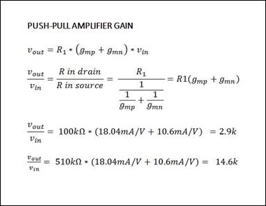
sourcing/sinking current. The amplifier gain is linearly related to the 100kΩ
resistor, as demonstrated in the theoretical calculations below. Consequently,
increasing the 100kΩ resistor to 510kΩ will result in a linear
increase in gain.
Theoretical Results
Again compare your hand calculations to simulation and
experimental results. Note that the gain of this amplifier is large so the
output may saturate at VDD and Ground. To avoid this saturation you can reduce
the AC input voltage using a voltage divider.
Simulation
Results
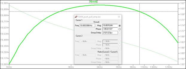
The 100kΩ
simulation using a 10mV input results in a gain of approximately 2.0k.
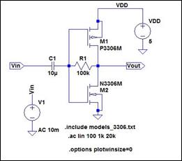
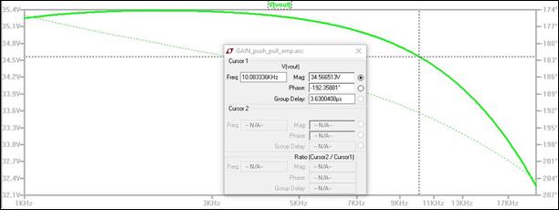
The 100kΩ
simulation using a 10mV input results in a gain of approximately 3.45k. Note
the saturation resulting in an inaccurate gain simulation. Using a voltage
divider in the simulations worked to reduce the gain,
however the gain still topped off at 3.45k and was thus not included in this
report.
Experimental
Results
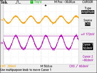
The gain with the 100kΩ resistor is displayed below. This
was obtained with 10 kΩ to 10Ω voltage divider at the input signal.
This resulted in an approximately 0.1mV input and a 432mV pk-pk
output. Dividing this by two and again by 0.1mV resulted in a gain of
approximately 2.16k. The laboratory oscilloscope will not display the 0.1mV at
the divider, so the measured value on Channel 1 is actually attached at the
input. I used the multi-meter to verify the AC signal at 0.1mV at the divider.
This yielded a signal in the vicinity, but not exactly 0.1mV. The same process
was repeated for the 510 kΩ experiment.
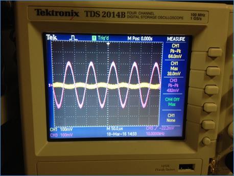
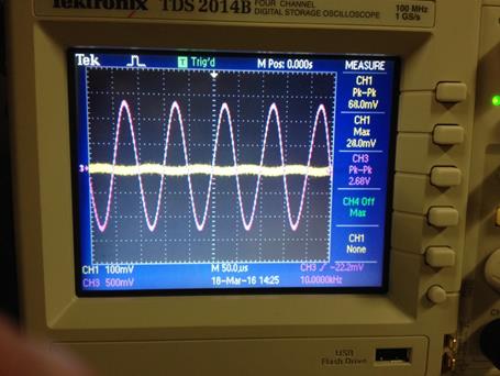
The gain with the 510kΩ resistor is displayed below. The
output is around2.68V pk-pk. Dividing
by 2 and again by 0.1mV results in a gain of approximately 13.3k.
|
NMOS |
Theoretical |
Simulation |
Experimental |
|
Gain |
2.86k |
1.99k |
2.16k |
|
PMOS |
|
|
|
|
Gain |
14.6k |
3.45k |
13.3k |
Conclusion
Laboratory experiment seven offered a comprehensive instruction in
single stage transistor amplifiers using the ZVN3306A and ZVP3306A amplifiers.
The basic topologies for the Common Drain, Common Source, Common Gate and
Push-Pull amplifiers and their respective gains, input resistances and output
resistances were all derived theoretically, simulated and experimentally
determined. The experiments and simulations offered insight into the practical
applications of each different topology and presented an opportunity to verify
how variables in each topology can be altered to manipulate the inherent
characteristics of each amplifier.
Return to
Monahan Lab Report Directory
Return to EE 420L
Spring 2016 Student Directory