EE 420L Engineering Electronics II - Lab 1
2/9/16
Lab
5: Op-amps III, the op-amp integrator
Experiment
1:
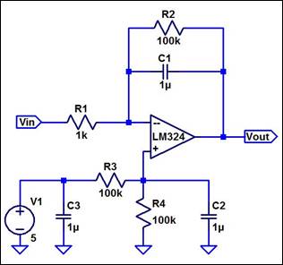
Calculate the frequency response of the following circuit. Ensure
you show your clear hand calculations.
The given circuit is
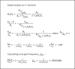
below to the left. Derivation of the frequency response via nodal analysis at
the negative terminal of the amplifier results in the calculations displayed in
the figure to the right.
What can you neglect to simplify the calculation?
To simplify the
calculation, R2 is neglected as shown in the calculations below. Essentially,
R1/R2 is much smaller than 1 and thus has a negligible impact on the circuit,
thus R2 can be neglected.
Does
the circuit work if you remove the 100k? Why or why not?
The circuit will still
work if the 100k resistor is removed if the op-amp behaves ideally, however
this is not likely. The likely result is the op-amp will have an offset voltage
and the 100k resistor is needed to compensate for the offset. If the 100k
resistor is removed and there is a DC offset at the input terminals, the output
will saturate or go to ground.
Does the 100k have much of an effect on the frequency response?
The 100k resistor does not have much of an effect on the frequency response as verified in the hand calculations below. A more intuitive explanation is the 100k resistor is too large for the AC current to flow through when a capacitor is a essentially a short for the current to flow through. Thus, the 100k resistor has a negligible impact on the frequency response.
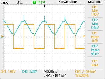
Verify your calculations with experimental results. Show, at the
unity-gain frequency of the integrator, that the input and the output have the
same peak values. Is the phase shift between
the input and the output what you expect? Why or why not?
The
image below displays the given circuit at the calculated unity-gain frequency.
The pulse input on channel 1 is scaled at 1.00V and displays approximately 3V pk-pk while the triangular output on channel 2 is scaled at
2.00V and displays approximately 3.00V pk-pk, as
well. I neglected to measure this more accurately with the cursors on the
oscilloscope, but the estimate holds visually. The phase shift between the
input and output measures 95![]() versus a theoretical phase shift of 90
versus a theoretical phase shift of 90![]() .
.
Experiment
2:
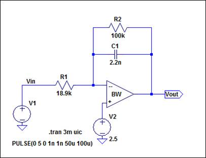
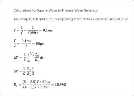
Next, design, simulate, and build a square-wave to triangle wave generation
circuit. Assume the input/output frequency is 10 kHz and the output ramp
must swing from 1 to 4 V centered around 2.5 V. Show all calculations and discuss the trade-offs (capacitor and
resistor values, input peak, min, and average, etc.)
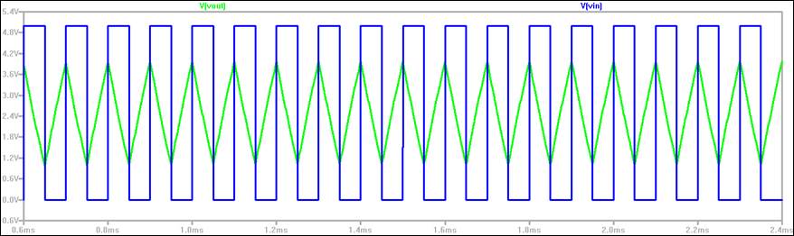
The design is based entirely from the circuit in experiment 1 above. The resistors and capacitors were decided upon based on the measured values of available capacitances in the laboratory. The goal was to choose a smaller capacitor to allow for a larger R1 to be used. This required solving for the necessary R1 to complete the circuit. A 100k resistor was utilized as in the first experiment to compensate for any offset voltage. The circuit design and the calculations are displayed in the figures below. The waveform below clearly indicates a pulse input with a triangular output centered around 2.5V and swinging from 1V to 4V at 10kHz.
Troubleshooting:
The simulation worked exactly as designed, however replicating these results in the laboratory experiment proved to be a challenge. The major issue confronted was an inability to produce the desired triangular waveform. The waveform the amplifier was putting out was almost a half triangle with a slight curve similar to a capacitor discharge. The circuit appeared to be connected properly and simple sources of potential error were systematically eliminated. These included improper connections, checking measured element values and replacing the LM324. The initial design parameters were changed with different values chosen and the same simulation results achieved, so the error definitely had to be in the experiment. Finally, the error was identified. The op-amp terminals were set to almost exactly 2.5VDC each when measured with a multi-meter. However, once the function generator was powered, the offset was not accounted for and the two input terminals were at different voltages when measured. This severely impacted the circuit. Once this issue was addressed and the correct offset was implemented on the function generator, the predicted waveform was generated, as shown below.
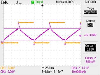
As seen in the above
waveform, the input pulse is 5V peak to peak and the output on channel 3 swings
from 1V to 4V with a ![]() of 3V at 10kHz. This was a satisfying
conclusion to a seemingly difficult issue.
of 3V at 10kHz. This was a satisfying
conclusion to a seemingly difficult issue.
Laboratory experiment five created an opportunity to systematically
design and implement an op-amp square-wave to triangle-wave generator and to
experiment with a classic op-amp design topology, namely the op-amp integrator.
The experiment also provided the ability to see how the integrator circuit
provides an output voltage proportional to the input voltage integrated over
time. The square-wave to triangle-wave generator demonstrated how simply
various elements within the design can be calculated to achieve a functioning
design set to operate within a given set of parameters.
Return to
Monahan Lab Report Directory