EE 420L Engineering
Electronics II - Lab 3
2/17/16
Lab 3: Op-amps I, basic
topologies, finite gain, and offset
This
lab will utilize the LM324 op-amp (LM324.pdf).
Review
the data sheet for this op-amp.
For
the following questions and experiments assume VCC+ = +5V and VCC- = 0V.
Knowing the non-inverting input, Vp, is at the same potential as
the inverting input, Vm, (called the common-mode
voltage, VCM) what are the maximum and minimum allowable common-mode voltages?
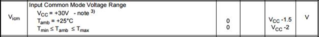
The datasheet for the LM324 indicates the common mode voltage,
VCM, has a maximum rating of (Vcc-1.5) and a minimum of 0V at room temperature
(+25![]() C). This is seen
in the image below directly from the LM324 datasheet. The Vcc
in the experiments is Vcc+ = +5V, thus the maximum
VCM is 5V - 1V = 3.5V. As seen on the datasheet and indicated in the footnote, Vcc+ is rated for a maximum of 30V.
C). This is seen
in the image below directly from the LM324 datasheet. The Vcc
in the experiments is Vcc+ = +5V, thus the maximum
VCM is 5V - 1V = 3.5V. As seen on the datasheet and indicated in the footnote, Vcc+ is rated for a maximum of 30V.
![]()
What is a good estimate for the op-amp's
open-loop gain? Support your answer with a plot from the datasheet and an
entry from the electrical characteristics table.
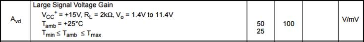
The
open-loop gain of an op-amp is the gain achieved when the circuit has no
feedback loop. An ideal op-amp has infinite open-loop gain. The LM324 datasheet
has several locations indicating open-loop gain.
Below
is the large signal voltage gain indicating a gain of 100V/mV or 100,000.
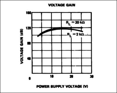
The
voltage gain graph to the left below gives the gain for different supply
voltages. The experiments in this laboratory exercise use Vcc+
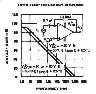
= +5V. This results in a gain estimate of approximately 100dB. The open-loop
frequency response graph indicates a gain of 100dB for frequencies around 10Hz.
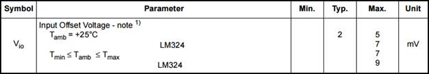
What is a good estimate for the offset
voltage? For worst case design what value would you use?
The
datasheet lists a typical offset voltage of 2mV with a maximum of 5V at room temperature,
thus 2mv is a good estimate for the offset voltage. For worst case design, the
9mV offset will be used to account for high temperature variations and provide
a large range for worst case scenarios.
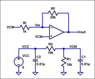
Build, and test, the following circuit.
Note that a precise value for the 5k resistors isn't important. You can
use 4.7k or a 5.1k resistors.
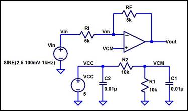
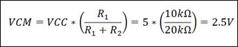
What is the common-mode voltage, VCM? Does VCM
change? Why or why not?
The
circuit above includes a voltage divider at DC, as both capacitors act as opens
at DC. Theoretically, VCM should be +2.5V as indicated below. The waveform
below the voltage divider calculation demonstrates VCM measures at
approximately 2.5V as indicated.

What is the ideal closed-loop gain?
The
circuit above has an inverting op-amp topology and thus has an ideal
closed-loop gain of ![]() This results in a unity gain 180
This results in a unity gain 180![]() out of phase with the input.
out of phase with the input.
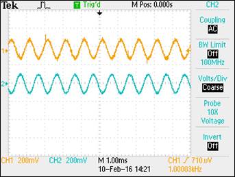
What is the output swing and what is it centered
around? What happens if the input isn't centered around VCM, that is, 2.5 V? Provide a detailed
discussion illustrating that you understand what is going on.
The
output swing is the range of voltage that an op-amp physically provides at its
output. As indicated in the ideal closed-loop gain calculation above, the
output will swing at the same amplitude as our input, 2.5V, but 180![]() out of phase. The waveform below displays the
output on channel 2 out of phase, but with the same amplitude as our input on
channel one.
out of phase. The waveform below displays the
output on channel 2 out of phase, but with the same amplitude as our input on
channel one.
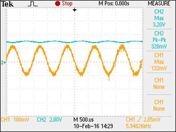
If
the input is not centered around VCM, the output
signal changes according to the value of the input. Initially, the same power
supply was used to power VCC and provide a constant DC voltage to the LM432,
but the result was VCM did not match Vm and we had no
AC signal riding the DC input and the output was clipped. The clipping resulted
from the output not swinging around 2.5V due to the output offset. This issue
was resolved by connecting one supply channel directly to VCC+ on the LM432 and
one to the voltage divider. The voltage at the divider was lowered until VCM
and Vm displayed equivalent input voltages. The
result was an output centered around 3.1V±132mV for an
output swing of 2.968V to 3.232V as shown below. This issue clearly
demonstrated the necessity of laboratory experimentation to demonstrate
practical application of theory.
What is the maximum allowable input signal
amplitude? Why?
The
maximum allowable input signal is 2.5V due to the maximum 5V VCC. Any signal
larger than 2.5V will be clipped because it will exceed the supply voltage.
What is the maximum allowable input signal if
the magnitude of the gain is increased to 10? Why?
Increasing
the gain by 10 means the input signal must be decreased by a factor of ![]() to 250mV. This is to account for the clipping
that occurs with respect to the rails. The calculation below demonstrates any
input larger than 250mV will result in clipping.
to 250mV. This is to account for the clipping
that occurs with respect to the rails. The calculation below demonstrates any
input larger than 250mV will result in clipping.
![]()
What is the point of the 0.01 uF capacitors from VCC and VCM to ground? Are these values
critical or could 0.1 uF, 1,000 pF, 1 uF, etc. capacitors be used?
The
capacitors act as coupling capacitors in this circuit. The coupling capacitors
separate the AC and DC components of a signal due to a capacitor acting as an
open to DC and a short to AC. They also prevent noise and help 'couple' the
output of one stage of the circuit to the input of the next stage to create a
stable circuit. The values of the capacitor are not critical because they are
only for decoupling and do not affect VCC or VCM since they are DC voltages.
The data sheet shows that this op-amp has an
input bias current that flows out of the op-amp's inputs of typically 20 nA. This current flows
out of both the non-inverting and inverting inputs through the resistors
connected to these inputs. Show how the operation of the circuit can be
effected if, for example, R1 and R2, are much larger. Explain what is going on.
The values of R1 and R2 can have a noticeable
impact on the circuit. The two resistors should ideally be the same value or
close to the same value to keep the output centered and allow for the largest
output swing possible. If the values of R1 and R2 are increased to much larger
values, the input bias current begins to impact the voltage divider circuit.
Specifically, the two terminals have two 5kΩ resistors in parallel with
20nA flowing through to ground, resulting in a voltage drop of 0.1mV. Adding
0.1mV to a VCM of 2.5V results in 2.6V and a signal that starts clipping due to
the signal exceeding the power supply limits. However, larger resistors will
result in a larger voltage added to VCM and a clipped output. For example 100MΩ
resistors results in 50MΩ*20nA and 1V added to VCM. This is a large
impact on circuit functionality.

Input
Bias Current LM324
What is the input offset current? What does this
term describe?
The
input offset current is the difference between the input bias currents of the
op-amp terminals.

Input Offset
Current LM324
Explain how the following circuit can be used
to measure the op-amp's offset voltage.
Note that if the output voltage is precisely the same as VCM then
the op-amp has no offset voltage (this is very possible).To measure small
offset voltages increase the gain by increasing RF to 100k or larger. Explain
what is going on.
The circuit above
applies the same input, VCM, to both the inverting and non-inverting inputs of
the op-amp. Assuming the op-amp to be ideal, no current flows through Rf because the nature of the
op-amp causes Vm at the inverting terminal to be
equivalent to VCM at the non-inverting terminal. Thus, performing circuit
analysis results in ![]() at the inverting terminal.
By Kirchhoff's Current Law, current entering a node equals current
exiting the same node and therefore, the current through Rf would be zero. Consequently, if there is an offset
voltage, Vm will equal VCM plus the offset voltage.
The inverting amplifier will amplify this differential by a factor of 20. To
measure the offset voltage, measure Vout and VCM,
calculate the difference between them and divide by a factor of 20. The result
will be the offset voltage.
at the inverting terminal.
By Kirchhoff's Current Law, current entering a node equals current
exiting the same node and therefore, the current through Rf would be zero. Consequently, if there is an offset
voltage, Vm will equal VCM plus the offset voltage.
The inverting amplifier will amplify this differential by a factor of 20. To
measure the offset voltage, measure Vout and VCM,
calculate the difference between them and divide by a factor of 20. The result
will be the offset voltage.
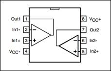
Measure the offset voltage of 4 different op-amps and compare
them.
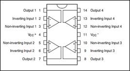
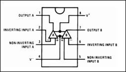
The four op-amps
measured and compared are the LM324, the TL-082, the LF351 and the LM393. The
pin connections (top view) and links to the datasheet for each op-amp are given
below.
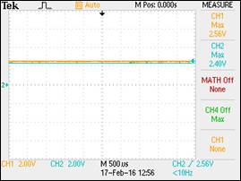
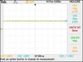
The measured values of VCM and Vout are given in the waveforms and tables below.
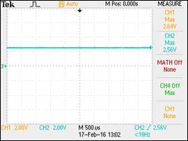
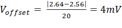
LM324
|
LM324 |
Volts |
|
VCM |
2.64 |
|
Vout |
2.56 |
|
Voffset |
4mv |
![]()
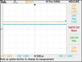
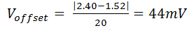
TL082
|
TL082 |
Volts |
|
VCM |
2.40 |
|
Vout |
1.52 |
|
Voffset |
44mv |
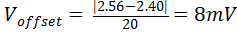
LF351
|
LF351 |
Volts |
|
VCM |
2.56 |
|
Vout |
2.40 |
|
Voffset |
8mv |
LM393
|
LF393 |
Volts |
|
VCM |
2.64 |
|
Vout |
2.56 |
|
Voffset |
8mv |
Each of the
op-amps measured had an offset voltage with the TL082 easily the largest at
44mV and the LM324 and LM393 the lowest at 4mV.
Conclusion
Laboratory
exercise three presented a synopsis on basic operational amplifier topologies,
specifically inverting and non-inverting topologies, as well as an opportunity
to relate the information on an op-amp's datasheet to the practical operation of
the amplifier in a circuit. Comprehending the relationships of parameters in
operational-amplifier circuits, such as common mode voltage, closed-loop gain,
output swing and maximum allowable input signal create the foundation for
learning to design with these multi-faceted devices. The experiments also
allowed insight into how attaching circuits to the op-amp terminals can allow
manipulation of the inherent characteristics of the op-amp to achieve a
specific design goal, such as the ability to measure the offset voltage via the
simple connection of VCM at both input terminals in experiment two.
Return to
Monahan Lab Report Directory
Return to EE 420L
Spring 2016 Student Lab Directory