EE 420L Engineering Electronics II - Lab 2
2/10/16
Lab 2: Operation of a Compensated Scope Probe
Perform,
and document in your html lab report, the following:
- Show scope waveforms of a 10:1 probe undercompensated,
overcompensated, and compensated correctly.
- Comment on where the type of scope probe (i.e., 1:1,
10:1, 100:1, etc.) is set on your scope (some scopes detect the type of
probe used automatically).
- Draft the schematic of a 10:1 scope probe showing: the
9 MEG resistor, 1 MEG scope input resistance, capacitance of the cable,
scope input capacitance, and capacitance in the probe tip.
- Using circuit analysis, and reasonable/correct values
for the capacitances, show using circuit analysis and alegbra
(no approximations), that the voltage on the input of the scope is 0.1 the
voltage on the probe tip.
- Devise an experiment, using a scope, pulse generator,
and a resistor, to measure the capacitance of a length of cable. Compare
your measurement results to the value you obtain with a capacitance meter.
Make sure you show your hand calculations.
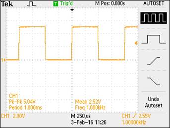
- Build a voltage divider using two 100k resistors.
Apply a 0 to 1 V pulse at 1 MHz to the divider's input. Measure, and show
in your report, the output of the divider when probing with a cable
(having a length greater than or equal to 3 ft)
and then a compensated scope probe. Discuss and explain the differences.
- Finally, briefly discuss how you would implement a
test point on a printed circuit board so that a known length of cable could
be connected directly to the board and not load the circuitry on the
board.
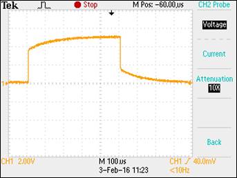
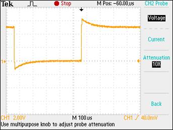
Experiment
1: Show scope waveforms of a 10:1 probe undercompensated, overcompensated,
and compensated correctly.
Undercompensated Probe Overcompensated
Probe
Compensated Probe
Experiment
2: Comment on where the type of scope probe (i.e., 1:1, 10:1,
100:1, etc.) is set on your scope (some scopes detect the type of probe used
automatically).
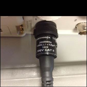
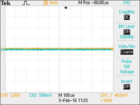
The type of scope probe is set in the channel menu for the Textronix
oscilloscope used in the experiment. The channel menu allows the user to choose
the proper attenuation for the type of probe being utilized. A probe fixed at a
10:1 attenuation was used throughout the experiment. The image on the left
below displays the 10X attenuation printed on the BNC connector, the 10MΩ
system input resistance, the typical input capacitance, 12pF, and the
bandwidth, 200MHz. The image on the right displays the menu for channel 2 with
the probe type set at 10X.
BNC Connector
10X Attenuation
The table below is
directly from the Tektronix website and offers a perspective on the range of
different values for the parameters mentioned above. Based on the table, the
model is possibly a P6117 or an earlier model of the same type.
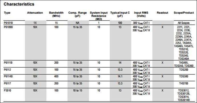
Source: Tektronix
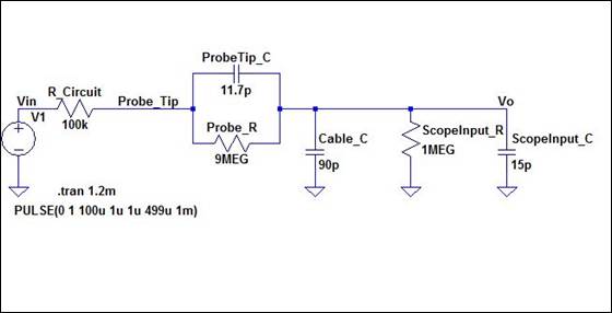
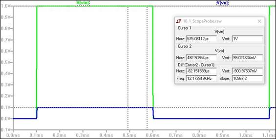
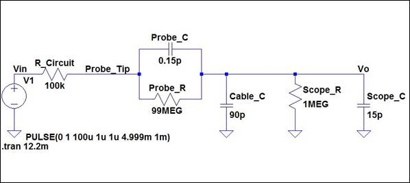
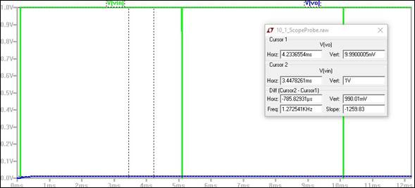
Experiment 3: Draft the schematic of a 10:1 scope probe showing: the 9
MEG resistor, 1 MEG scope input resistance, capacitance of the cable, scope
input capacitance, and capacitance in the probe tip.
The
10:1 probe schematic below displays the circuit utilized to gain the
attenuation necessary to account for the probe effect on the circuit. Running
the same simulation as demonstrated in the pre-lab video resulted in the waveform
to the right of the circuit. The pulse input from 0V to 1V results in an output
of approximately 100mV. This validates the proper compensation has been
achieved by the circuit.
Schematic 10:1
Probe 10:1
Probe Waveform
Using
the same techniques outlined for creating a 10:1 probe, the schematic below
displays a 100:1 scope probe with the resulting waveform. As expected, the
pulse output from 0V to 1V results in an output of approximately 10mV.
Schematic 100:1
Probe 100:1
Probe Waveform
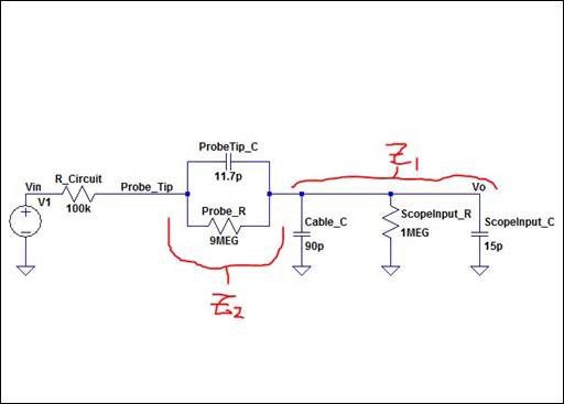
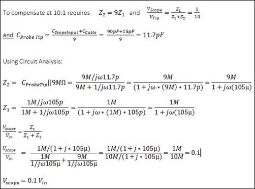
Experiment 4: Using circuit analysis, and reasonable/correct values for
the capacitances, show using circuit analysis and alegbra
(no approximations), that the voltage on the input of the scope is 0.1 the voltage
on the probe tip.
The circuit analysis and algebra demonstrating the voltage
on the input of the scope is equivalent to 0.1 the voltage on the probe tip.
Calculations are performed assuming a scope input capacitance of 15pF and a
cable capacitance of 90pF. The image on the left displays the circuit with
impedances in parallel circled and labeled to correlate with the calculations
displayed in the image on the right.
Circuit with
Labeled Impedances
Circuit Analysis
Experiment 5: Devise an experiment, using a scope, pulse generator, and a
resistor, to measure the capacitance of a length of cable. Compare your
measurement results to the value you obtain with a capacitance meter. Make sure
you show your hand calculations.
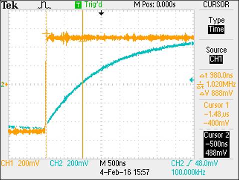
The simplest experiment to measure the capacitance of the
cable is to create a simple RC circuit using the scope probe and cable as the
capacitor in series with a resistor measured at 108kΩ. Using a voltage
pulse, ![]() as input and
measuring the time the output of the circuit takes to reach 50% of
as input and
measuring the time the output of the circuit takes to reach 50% of ![]() , known as the delay
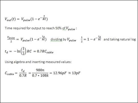
time, allows derivation of the capacitor value through the relationships
displayed in the calculations in the center image. The image to the left below
is the oscilloscope waveform for the simple RC circuit displaying a measured
delay time of 980.0ns for a 1V input pulse at 100kHz.
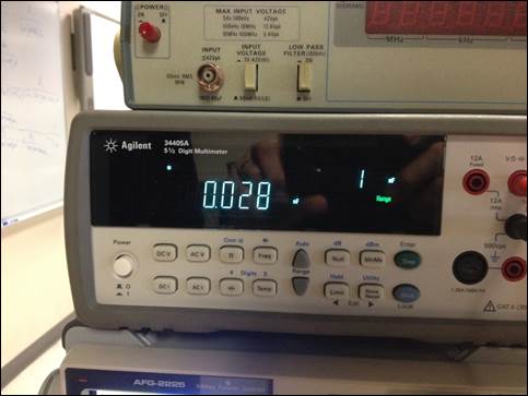
Using the measured time delay resulted in a calculated value of 13pF. Measuring
the cable capacitance with a multi-meter resulted in a value of 28pF. This is
higher than the calculated value obtained, but may be due to variations in the
different methods of measuring. For example, the probes used to measure the
cable capacitance on the meter are long cables with their own capacitance that
varies depending on how far apart or close they are held to one another.
, known as the delay
time, allows derivation of the capacitor value through the relationships
displayed in the calculations in the center image. The image to the left below
is the oscilloscope waveform for the simple RC circuit displaying a measured
delay time of 980.0ns for a 1V input pulse at 100kHz.
Using the measured time delay resulted in a calculated value of 13pF. Measuring
the cable capacitance with a multi-meter resulted in a value of 28pF. This is
higher than the calculated value obtained, but may be due to variations in the
different methods of measuring. For example, the probes used to measure the
cable capacitance on the meter are long cables with their own capacitance that
varies depending on how far apart or close they are held to one another.
Delay Time of RC
Circuit
Cable Capacitance Derivation
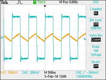
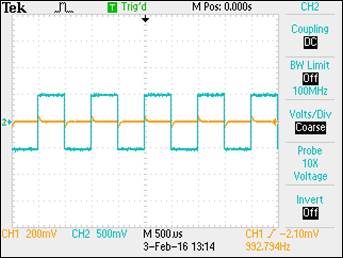
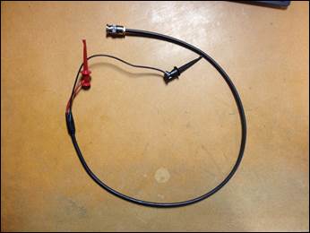
Experiment 6: Build a voltage divider using two 100k resistors. Apply a
0 to 1 V pulse at 1 MHz to the divider's input. Measure, and show in your
report, the output of the divider when probing with a cable (having a length
greater than or equal to 3 ft) and then a compensated
scope probe. Discuss and explain the differences.
The waveform on the left below displays the input and
output of the voltage divider when probing the output using a compensated
probe. The center image displays the output measured with an uncompensated
cable, pictured in the image on the right. The compensated probe has a 10:1 attenuation
and results in approximately 100mV output for a 1V input. This is due to the
compensation that reduces the capacitance introduced to the circuit and the
small RC resulting in the capacitor taking less time to charge and thus
allowing for a measurable signal. The
uncompensated probe results in a large capacitance being introduced to the
circuit with a resulting RC constant that is high and difficult to measure due
to the extended time necessary for the introduced capacitance to fully charge.
This is demonstrated by the nearly linear output in the center image. The cable
is effectively acting as a wire.
Compensated
Probe
Uncompensated Cable Actual Cable used
in Experiment 6
Experiment 7: Finally, briefly discuss how you would implement a test
point on a printed circuit board so that a known length of cable could be
connected directly to the board and not load the circuitry on the board.
A test point can be implemented on a PCB such that a
resistor and a variable capacitor in parallel are included in the circuit
design process to prevent any effects that would occur when a known length of
cable is attached to the test point. Essentially, the probe compensation is
included in the circuit design and would allow probing with the uncompensated
cable while minimizing the impact of the scope input and cable capacitance on
the circuit operation.
Conclusion
Laboratory experiment two introduced the topic of scope
probe compensation and an opportunity to learn about the techniques involved in
compensating scope probes, as well as the effects compensated and uncompensated
scope probes have on circuits. The influence uncompensated scope probes have on
circuits by introducing large capacitances and altering circuit operation can
be minimized by designing a circuit to compensate for the scope input
capacitance and cable capacitance. This includes a resistor and capacitor in
parallel at the tip of the probe calculated via a basic voltage divider to
reduce the capacitance introduced to the circuit and allow for a faster signal.
The result of laboratory experiment two is a more insightful comprehension of
the impact a measuring device can have on a circuit.
Return to
Monahan Lab Report Directory
Return to EE420L
Spring 2016 Student Directory