EE 420L Engineering Electronics II Lab - Lab 9
Design of a Beta-Multiplier Reference (BMR) using the CD4007 CMOS transistor array
Authored by Sergio Covarrubias
covars1@unlv.nevada.edu
04/15/2016
Part 1 (Pre-lab work)
Pre-lab work
- This lab will use the level=1 MOSFET model created in lab 8 and, again, the MOSFETs in the CD4007.pdf CMOS transistor array.
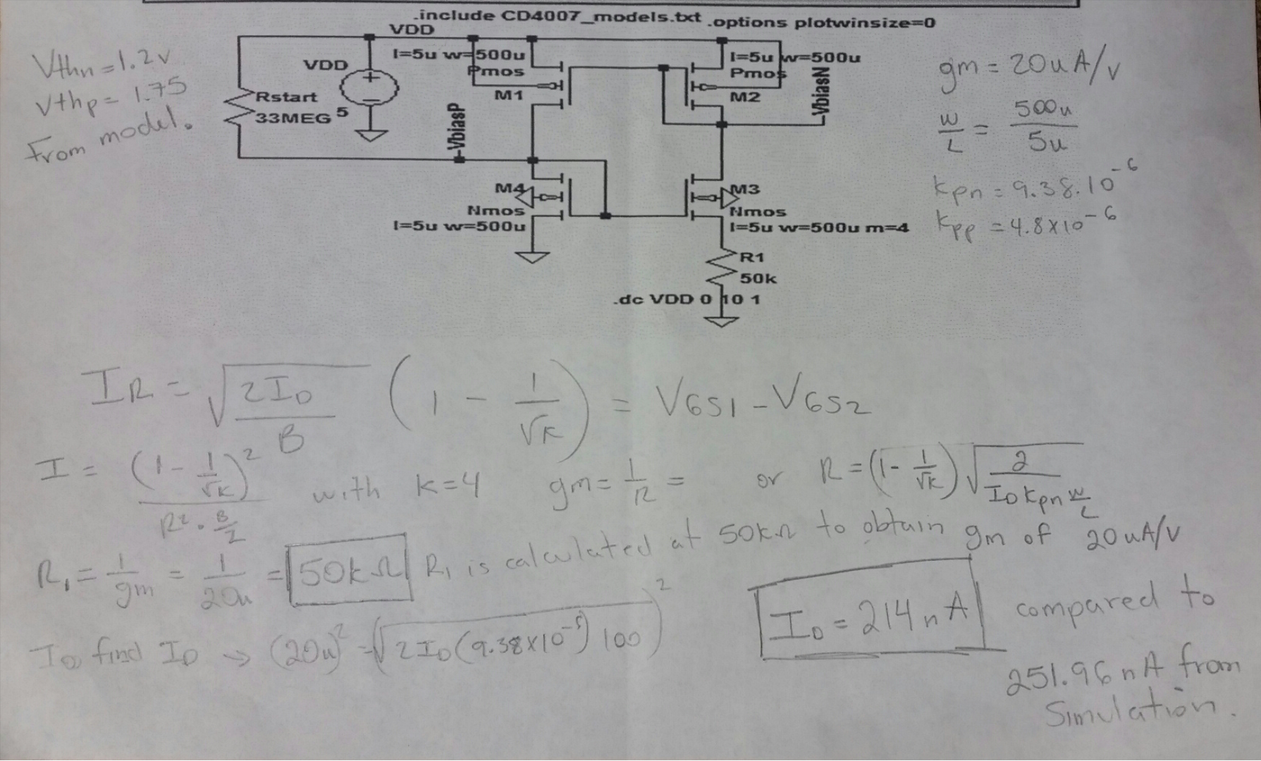
- Design and simulate the operation of a BMR that biases the NMOS devices so that they have a gm of 20 uA/V
- Use a simple (big) resistor to VDD for the start-up circuit (explain how the addition of a resistor ensures start-up).
- When
the BMR is operating the current in the big resistor should be much
smaller than the current flowing in each branch of the BMR
- Write-up,
similar to a homework assignment, your design calculations and
simulation results. (This will count as the pre-lab quiz.)
- Ensure that you show the following in what you turn in:
- Hand calculations
- Operation as VDD is swept from 0 to 10 V
- Vbiasn
should stabilize (be constant) after VDD hits a minimum value (estimate
this value of VDD assuming VGS/VSG is a threshold voltage and
VDS,sat/VSD,sat is zero).
- Vbiasp should follow VDD after VDD hits a minimum value (show this in simulations)
- Unstable operation if too much capacitance is shunting the BMR's resistor (see bottom of page 630)
- Comments comparing the hand calculations with the simulation results
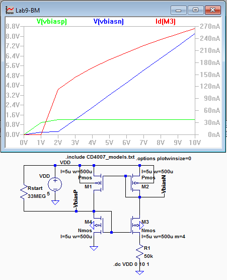

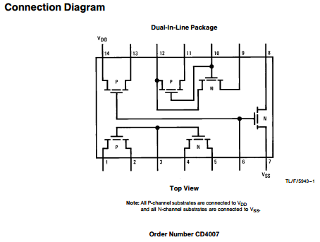
For
this lab we worked the LTspice simulation and calculations as a pre-lab
which made it easier in the actual lab, using my prelab BMR design I
built my circuit. I used the LEVEL=1 mosfet model that was used
in the previus lab#8. This design biases NMOS devices with produce a
gm=20uA/v and also I use a big resistor connected to Vdd which is used
as the START-UP circuit.
Part 2 (BMR build and current mirrors)
In this lab you may need to use two,
or more, CD4007 chips from the same production lot (see date code on
the top of chip) to ensure using a BMR to bias a current mirror is
possible. If the CD4007 chips are not from the same production lot they
will not "match" so current mirrors will not be possible.
- Build your BMR design and characterize it as you did in the pre-lab
- You
expect the BMR to become unstable if there is a large capacitance
across the resistor, such as a scope probe (important), so care must be
exercised
- Use your BMR to bias, and thus create, a:
- NMOS current mirror
- PMOS current mirror
- Measure how the current varies through each current mirror as the voltage across the mirror changes.
- Of
course the current in the NMOS (PMOS) current mirror goes to zero as
the voltage on the drain of the output device moves towards ground (VDD)
- Using these current mirrors drive two gate-drain connected transistors
- For the first experiment use the NMOS current mirror to drive two PMOS gate-drain connected devices.
- Use
the voltages on the gate-drain connection of the two devices to bias a
cascode current mirror (characterize this mirror as before)
- For the second experiment switch, that is, use the PMOS current mirror to drive two NMOS gate-drain connected devices.
- Again, use these two voltages to bias an NMOS cascode current mirror then characterize.
Part 2.1 (BMR)
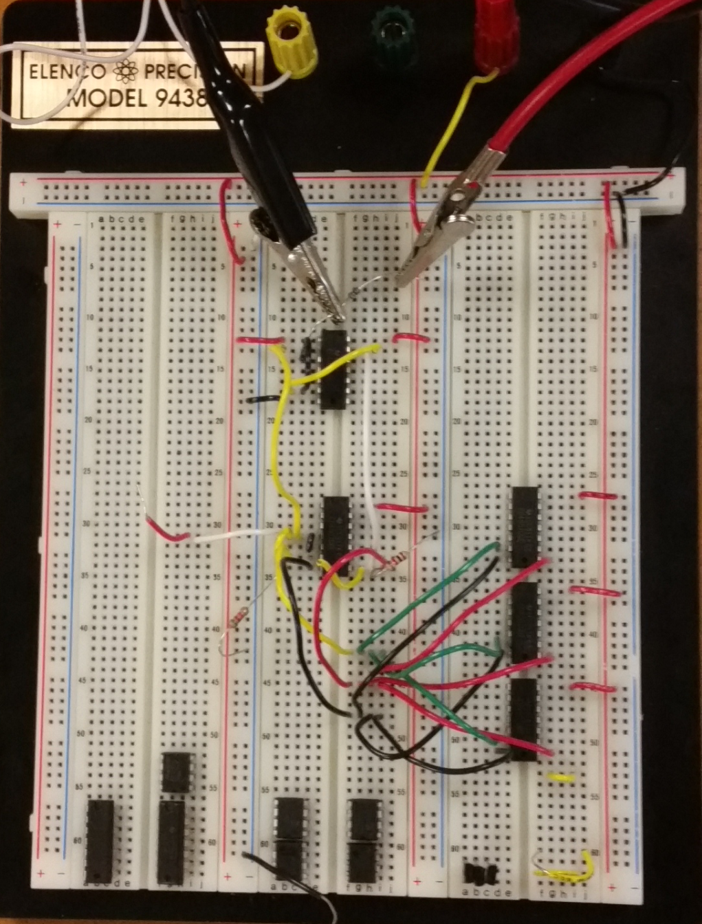
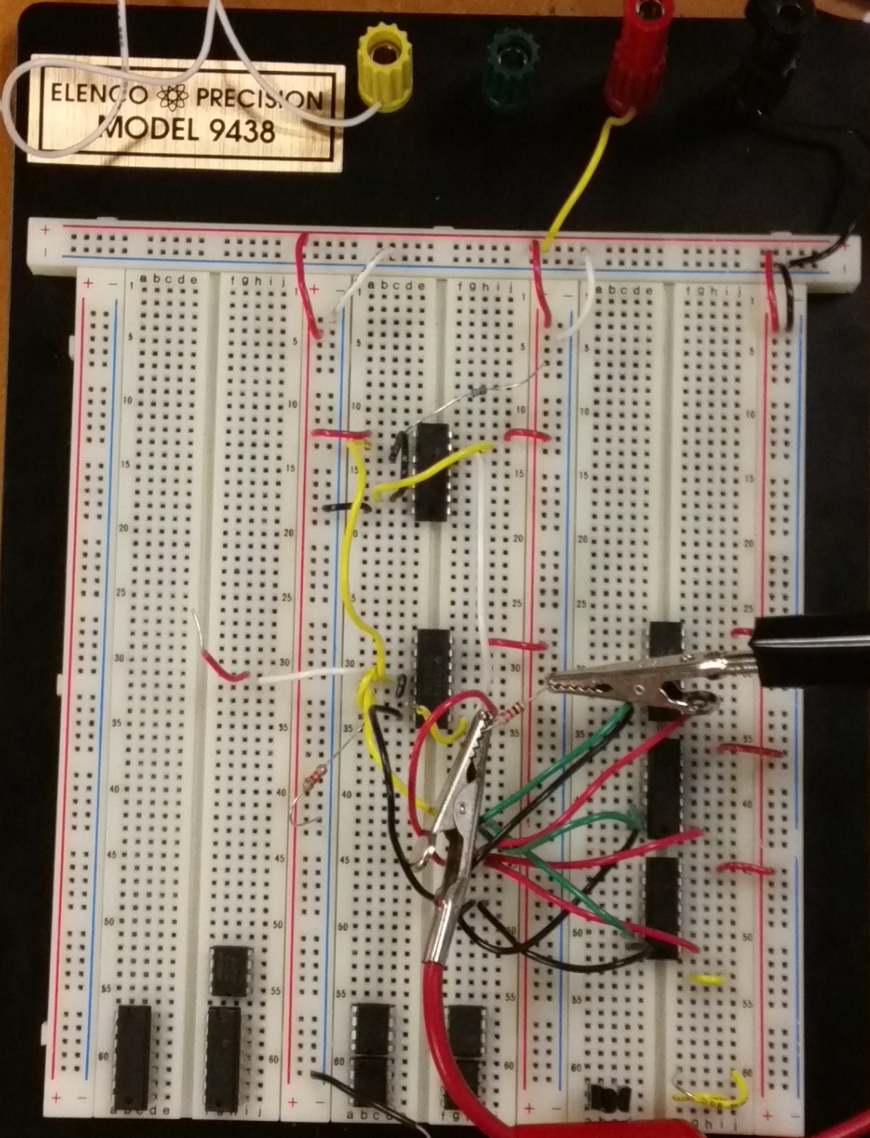
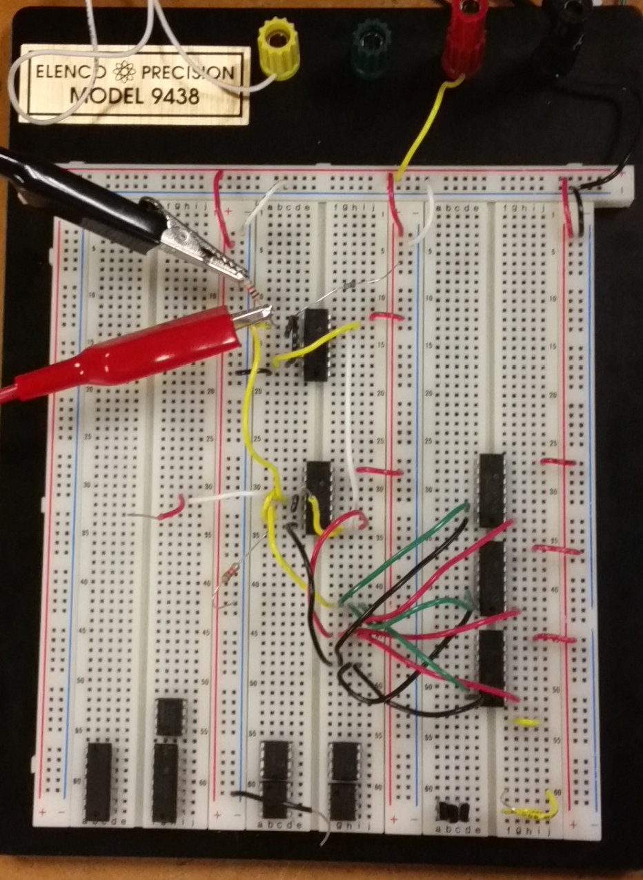
| BMR | BMR CIRCUIT BUILD |
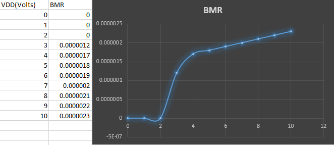 |  |
For
this experiment to calculate the current I measured the voltage across
the R1 50 ohm resistor, the generated curve behaves almost as expected
expect that it does not flatten out but insted it continues to go up as
voltage increases. This circuilt was challenging to build because the
position of the nmos and pmos in the CD4007 chip, I have to check it
over and over again until I found a mistake o my wiring which was
giving completelly wrong voltages.
Part 2.2 (NMOS)
| NMOS CURRENT MIRROR | Nmos Circuit Build |
 |  |
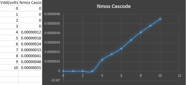
| NMOS CASCODE CURRENT MIRROR |
 |
Part 2.3 (PMOS)
| PMOS CURRENT MIRROR | Pmos Circuit Build |
 |  |
| PMOS CASCODE CURRENT MIRROR |
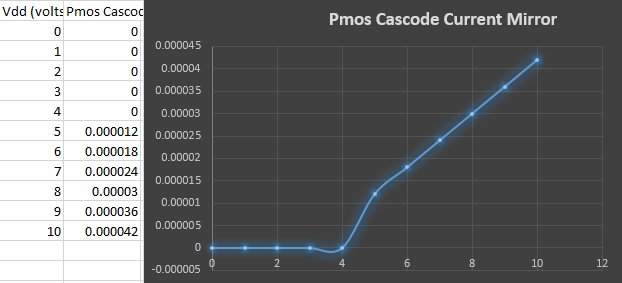 |
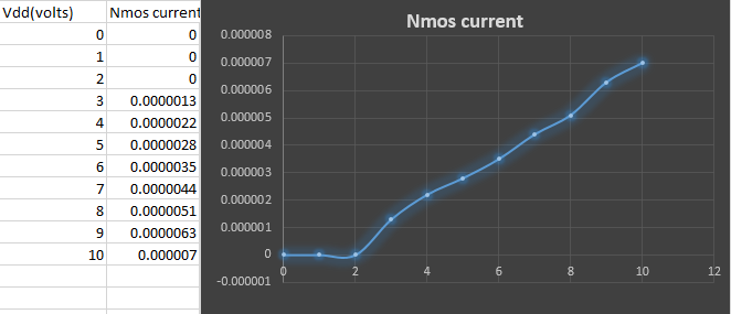
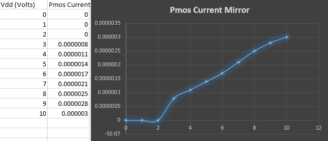
Comparing
the curve shapes of my PMOS and PMOS currents I was able to show a
simillar shape, but my values were off at a higher values. I noticed
that using resistors of same values I kept getting different results
which proved that the resistors vary a lot even on identical resistors.
Also the CD4007 chips will make the results vary as they are not
identically made. Over all I was happy with my results as I was able to
see the Pmos ad Nmos properties and actual behavior.
Return to COVARS1 Homepage
Return to EE 420L Labs
