EE 420L Engineering Electronics II Lab - Lab 8
Characterization of the CD4007 CMOS transistor array
Authored by Sergio Covarrubias
covars1@unlv.nevada.edu
04/10/2016
Pre-lab work
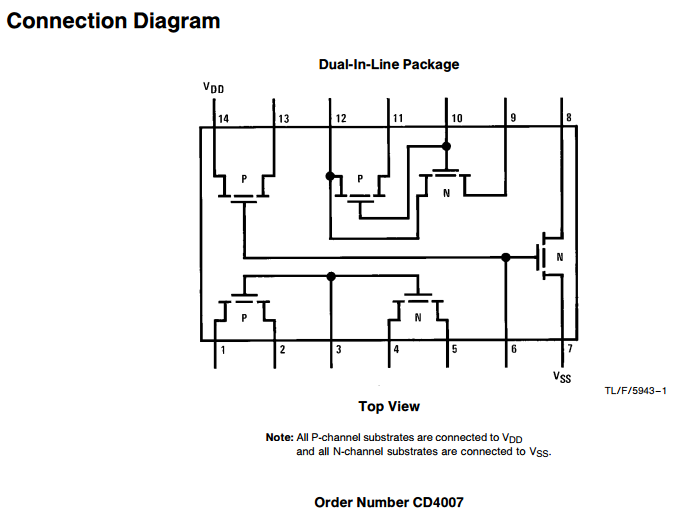
- Review the datasheet for the CD4007.pdf CMOS transistor array.
- Ensure
that you understand how the bodies of the NMOS are tied to pin 7 (VSS,
generally the lowest potential in the circuit, say ground) and that the
bodies of the PMOS are tied to pin 14 (VDD, generally the highest
potential in the circuit, say + 5V).
In
this lab you will characterize the transistors in the CD4007 and
generate SPICE Level=1 models. Assume that the MOSFETs will be used in
the design of circuits powered by a single +5 V power supply. In other
words, don't characterize the devices at higher than +5 V voltages or
lower than ground potential.
- Experimentally generate, for the NMOS device, plots of:
- ID v. VGS (0 < VGS < 3 V) with VDS = 3 V
- ID v. VDS (0 < VDS < 5 V) for VGS varying from 1 to 5 V in 1 V steps, and
- ID v. VGS (0 < VGS < 5 V) with VDS = 5 V for VSB varying from 0 to 3 V in 1 V steps.
- Note
that for this last one, if VSS (NMOS body) is ground (again, the
Body, VB, is grounded) then the source voltage will be varied from 0 to
3 V in 1 V steps to realize VSB ( = VS - VB = VS) varying from 0 to 3 V
in 1 V steps. At the same time VGS will be varied from 0 to 3 V (when
VS = 0), 1 to 4 V (when VS = 1 V), 2 to 5 V (when VS = 2 V), and 3
to 5 V (when VS = 3 V). In other words, as VS is increased by 1 V the
VGS has to shift up by 1 V as well.
- Assuming
that the length of the NMOS is 5 um and its width is 500
um calculate the oxide thickness if Cox (= C'ox*W*L) = 5 pF.
- From this measured data create a Level = 1 MOSFET model with (only) parameters: VTO, GAMMA, KP, LAMBDA, and TOX.
- Compare
the experimentally measured data above (the 3 plots) to
LTspice-generated data (again, 3 plots) and adjust your model
accordingly to get better matching.
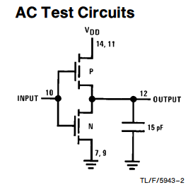
- Experimentally,
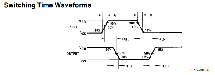
similar to what is seen on the datasheet (AC test circuits seen on page
3 of the datasheet), measure the delay of an inverter using these
devices (remember the loading of the scope probe is around 15 pF and
there is other stray capacitance, say another 10 pF).
- Using
your model simulate the delay of the inverter and compare to measured
results. Adjust your SPICE model to get better matching between the
experimental data and the measured data.
- Repeat the above steps for the PMOS device where VDS, VGS, and VSB are replaced with VSD, VSG, and VBS respectively.
Ensure
that your html lab report includes your name, the date, and your email
address at the beginning of the report (the top of the webpage).
When finished backup your work.
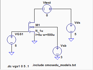
CD4007 Chip used for this Lab
NMOS
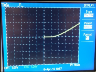
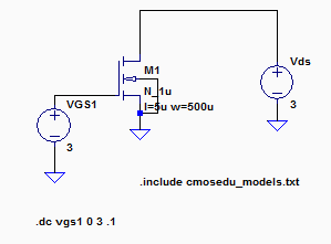
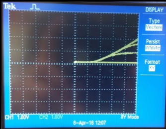
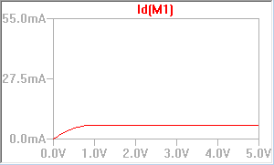
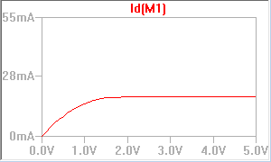
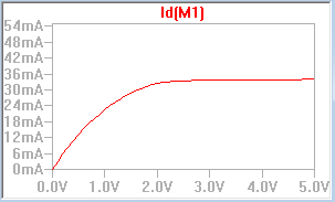
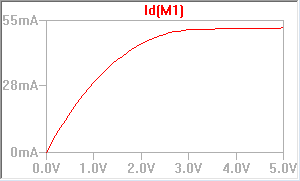
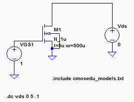
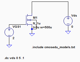
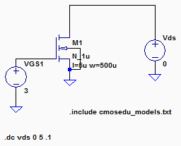
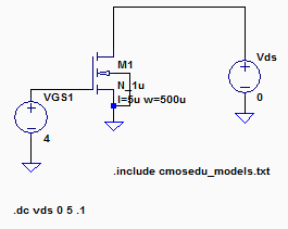
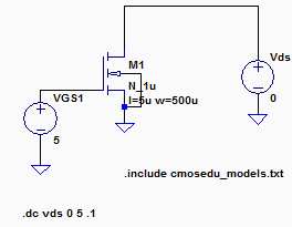
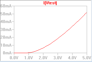
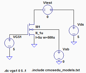
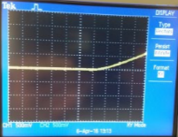
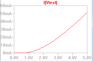
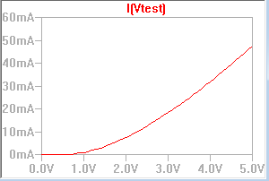
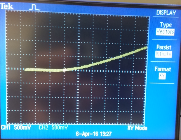
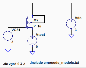
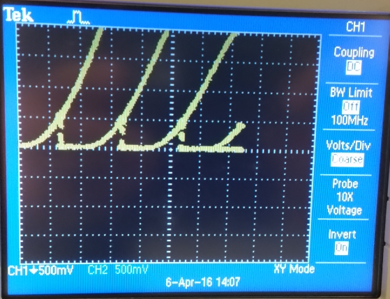
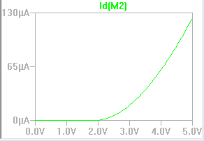
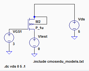
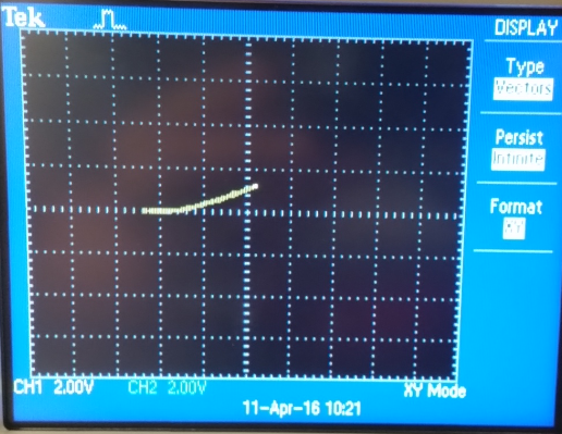
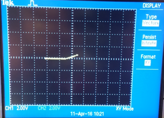
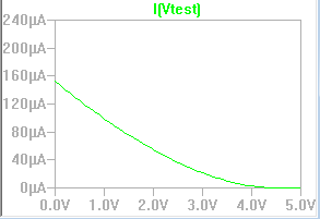
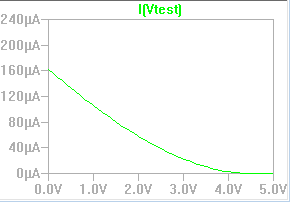
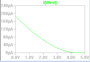
Part 1- ID v. VGS (0 < VGS < 3 V) with VDS = 3 V
From the data sheet we know that this NMOS is 5um with a width of 500um to calculate the oxide thickness Cox'.
Cox=C'ox*W*L=5pf
Cox'=(5pF)/(5u*500u)=0.002
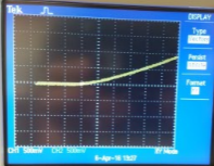
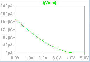
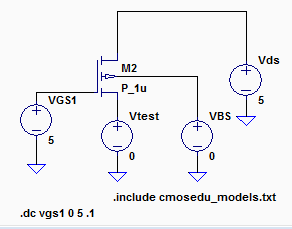
| Osiloscope screen capture. | LTSpice Simulation Graph | LTSpice Circuit | Calculations |
 | 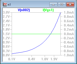 |  | From the data sheet we know that this NMOS is 5um with a width of 500um to calculate the oxide thickness Cox
Cox=C'ox*W*L=5pf
Cox'=(5pF)/(5u*500u)=0.002 |
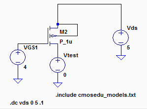
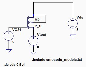
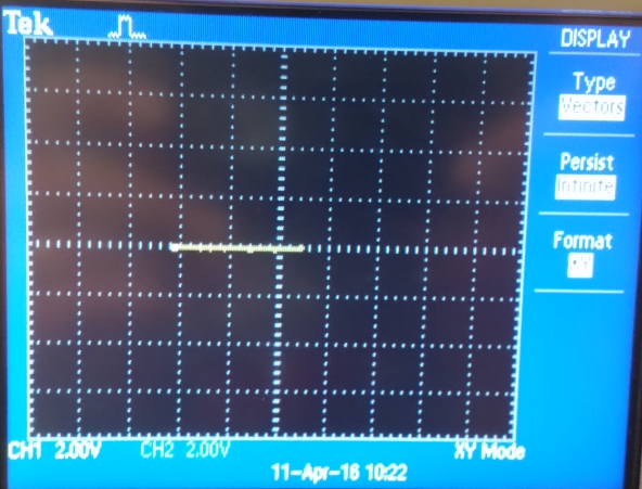
Part 2- ID v. VDS (0 < VDS < 5 V) for VGS varying from 1 to 5 V in 1 V steps
| Osiloscope screen capture. |
LTSpice Simulation Graph | LTSpice Circuit |
 | VGS at 1V
VGS at 2V
VGS at 3V
VGS at 4V
VGS at 5V
 | VGS at 1V
VGS at 2V
VGS at 3V
VGS at 4V
VGS at 5V
 |
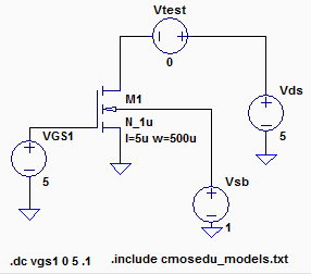
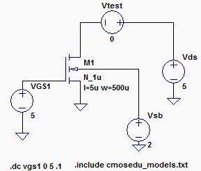
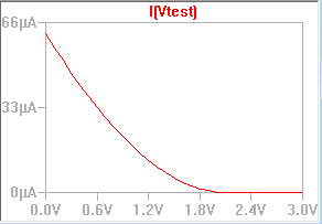
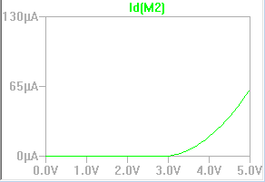
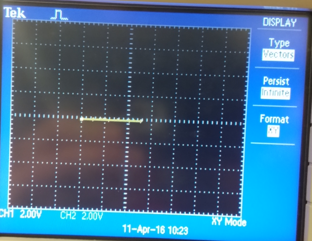
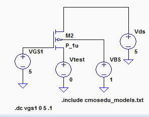
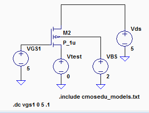
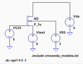
Part 3- ID v. VGS (0 < VGS < 5 V) with VDS = 5 V for VSB varying from 0 to 3 V in 1 V steps.
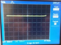
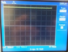
| Osiloscope screen capture. | LTSpice Simulation Graph | LTSpice Circuit |
V=0 volts
 |  |  |
V=1 volts.
|  |  |
V=2 volts
|  |  |
V=3 volts
 |  |  |
PMOS
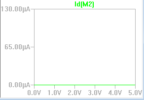
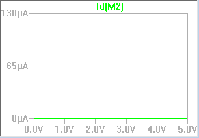
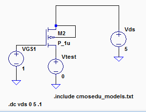
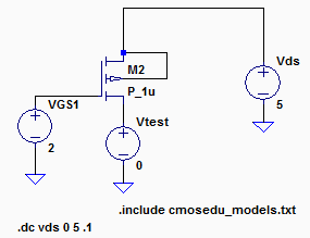
Part 1- ID v. VGS (0 < VGS < 3 V) with VDS = 3 V
| Osiloscope screen capture. | LTSpice Simulation Graph | LTSpice Circuit |
 |  |  |
Part 2- ID v. VDS (0 < VDS < 5 V) for VGS varying from 1 to 5 V in 1 V steps
| Osiloscope screen capture. | LTSpice Simulation Graph | LTSpice Circuit |
 | VGS1 = 1V
VGS1 = 2V
VGS1 = 3V

VGS1 = 4V
VGS1 = 5V
 | VGS1 = 1V
VGS1 = 2V
VGS1 = 3V
VGS1 = 4V
VGS1 = 5V
 |
Part 3- ID v. VGS (0 < VGS < 5 V) with VDS = 5 V for VSB varying from 0 to 3 V in 1 V steps.
| Osiloscope screen capture. | LTSpice Simulation Graph | LTSpice Circuit |
VBS=0v
VBS=1v
VBS=2v
VBS=3v
 | VBS= 0v
VBS= 1v
VBS= 2v
VBS= 3v
 |
VBS= 0v
VBS= 1v
VBS= 2v
VBS= 3v
 |
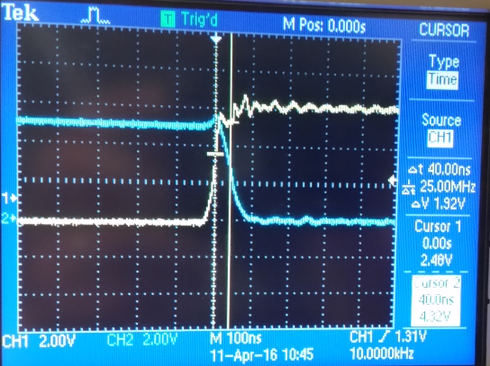
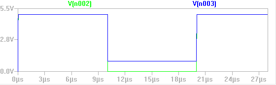
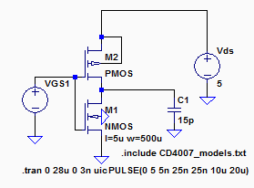
INVERTER
Using the CD4007 chip we can also construct an inverter.
My experimental delay is 40nS.
| Osiloscope screen capture. | LTSpice Simulation Graph | LTSpice Circuit |
 | 
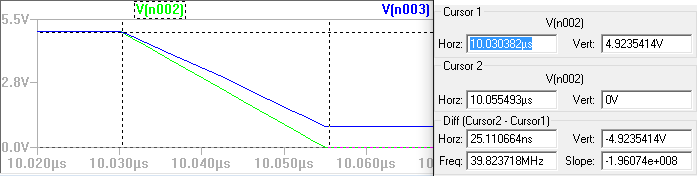 |  |
On LTspice the inverter delay is 25.11nS which is in the ballpark as specified in the range on the datasheet of the CD4007.
Return to COVARS1 Homepage
Return to EE 420L Labs