Lab 3 - EE 420L
This lab will utilize the LM324 op-amp (LM324.pdf).
Review the data sheet for this op-amp.
For the following questions and experiments assume VCC+ = +5V and VCC- = 0V.
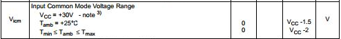
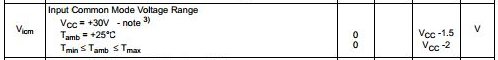
Knowing the non-inverting input, Vp, is at the same potential as the inverting input, Vm, (called the common-mode voltage, VCM) what are the maximum and minimum allowable common-mode voltages?
Support your answer with an entry from the electrical characteristics table in the datasheet.
What is a good estimate for the op-amp's open-loop gain?
Support your answer with a plot from the datasheet and an entry from the electrical characteristics table.
What is a good estimate for the offset voltage?
For worst case design what value would you use?
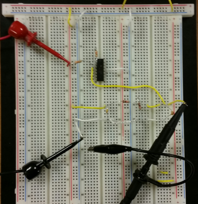
Build, and test, the following circuit. Note that a precise value for the 5k resistors isn't important. You can use 4.7k or a 5.1k resistors.
What is the common-mode voltage, VCM? Does VCM change? Why or why not?
What is the ideal closed-loop gain?
What is the output swing and what is it centered around?
What happens if the input isn't centered around around VCM, that is, 2.5 V?
Provide a detailed discussion illustrating that you understand what is going on.
What is the maximum allowable input signal amplitude? Why?
What is the maximum allowable input signal if the magnitude of the gain is increased to 10? Why?
What is the point of the 0.01 uF capacitors from VCC and VCM to ground?
Are these values critical or could 0.1 uF, 1,000 pF, 1 uF, etc. capacitors be used?
The data sheet shows that this op-amp has an input bias current that flows out of the op-amp's inputs of typically 20 nA.
This current flows out of both the non-inverting and inverting inputs through the resistors connected to these inputs.
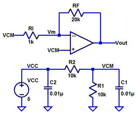
Show how the operation of the circuit can be effected if, for example, R1 and R2, are much larger. Explain what is going on.
What is the input offset current? What does this term describe?
The non-inverting input "Vp" is at the same potential as the inverting input "Vm". From the data sheet we need to know the commonmode voltage "VCM" .
what are the maximum and minimum allowable common-mode voltages?
Maximum common mode voltage 5V-1.5v=3.5V
Minimum common mode voltage =0V
The open loop gain is typically 100V/mV which is equal to 100k V/V.
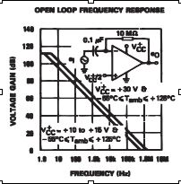
and also from the data sheet we know that: 20log(x) = 100, x = 5, 10e5 = 100k V/V.
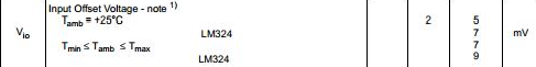
From the information given in the data sheet we can see that the average offset voltage is 2mV.
The and for a worst case senerio we have a maximum value of 9mV.
For the first experiment we will use this ciruit:
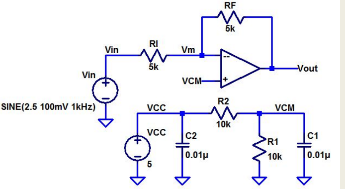
VCM=2.5V
The 2.5V will not change, the capacitors act as an AC short.
If there is any variation it will discharge in the capacitors and 2.5v DC will be unchanged.
The DC gain is 1, We have +2.5V on the non inverting ternimal and -2.5V at the inverting terminal.
Because bought terminals are the same our gain is 1 V/V.
The AC gain is -1 because the AC source goes into the inverting terminal and the non inverting terminal is 0v.
The op-amp is in the inverting topology which means our gain is:
-R2/R1 = -5k/5k = -1.
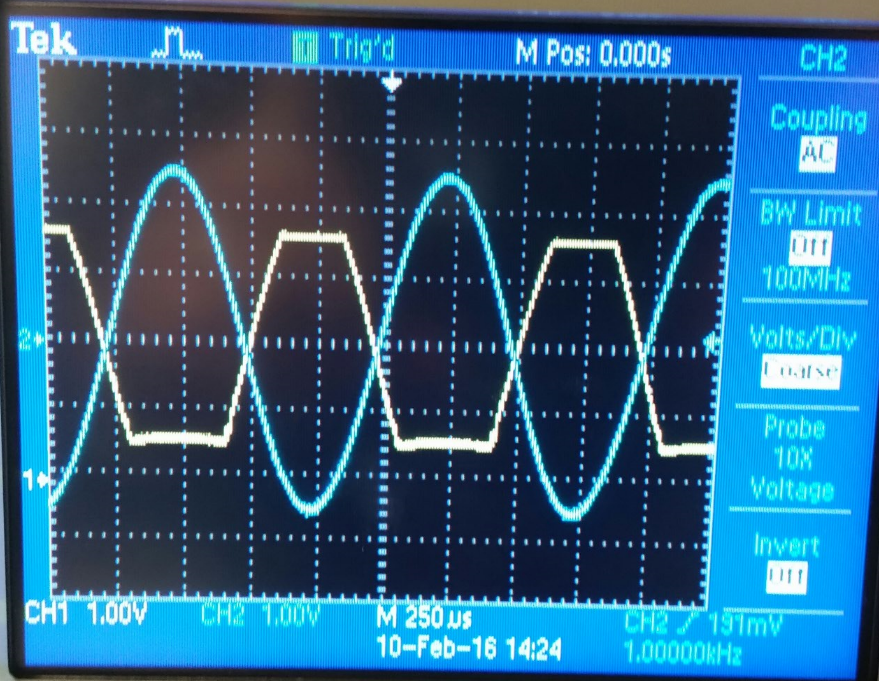
The output swing will be centered at 2.5V (VCM) and the AC signal the output swing is 100mV. If we do not center our swing at 2.5v we will not be able to see it and could go to saturation.
Our amplitude goes between Vcc = 5 and -Vcc = 0, out output will only swing between those two values. If our ouput goes outside these boundaries our signal will saturate and it will clip off. Our center is at 2.5 and it will go +-2.5.
For the top boundary 2.5 + 2.5 = 5.
And for the lower boundary-2.5 + 2.5 = 0.
The gain is -1 which tells us the maximum input signal is 2.5v.
If our gain is increased to 10, we can still only swing between Vcc = 5 and -Vcc = 0. And because we are centered at 2.5V, our signal can only swing 2.5V. This means our max input is (input) x 10 = 2.5 which makes our max input signal 250mV.
The capacitor are only there act as a short for any AC wiggle and keep our input as 2.5VDC.
The sizes of the capacitor are not really important but we want the values to be as small as posible to prevent any DC voltage lost.
The input bias current flows out of our inverting and non-inverting terminals. The current also flows through the resistors.
In our experiment the resistor R1 and R2 are 5k.
20nA*(5k || 5k) = 50uV, which makes our VCM 2.5V + 50uV
If the resistors were larger like 50K
20nA*(50k || 50k) = 0.5mV, which makes our VCM 2.5V + 0.5mV
The change in the resistors afects the VCM but not too much.
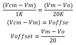
offset voltage = (|Vp-Vm|)/A
Vm = voltage at inverting terminal
Vp = voltage at non-inverting terminal
and A = gain.
We will use this formula to calculate the offset voltage of four different op-amps (showed in the table below).
OP-Amp #1 MPC601 | OP-Amp #2 LF353N |
| Vm=2.4947V Vo =2.4935V 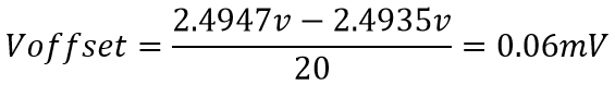 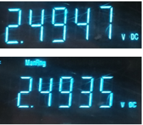 | Vm=2.6796V Vo=2.4935V 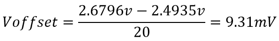 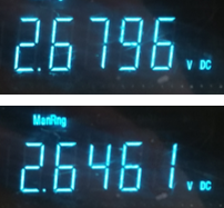 |
OP-Amp #3 TL081 | OP-Amp #4 MAX7414 |
| Vm=2.3612V Vo=2.3338V 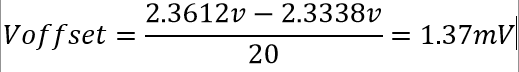 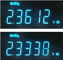 | Vm=2.4950V Vo=2.4901V 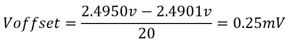 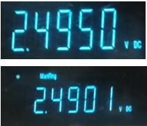 |