Final Project - EE 420L
Goal/Purpose:
To have a
voltage references that is not affected by power supply voltage (with constrain
of Vref<VDD), temperature and process variation. In order to accomplish these different
methods can be applied, but the one we used was with parasitic Diode Based
Reference. Because of the chips restrictions we did not use a beta multiplier,
but a DBR.
Theory:
If the reference
voltage increases with temperature the Vref is PTAT, and if it decreases is said to be CTAT.
This combined together to give a small change in voltage reference. This kind
of voltage reference is called band gap reference. For this circuit DBR is
used.
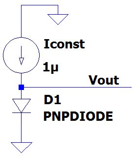
First Step is to
get the diodes characterization
base on the model
provided by diodes.com we got this spice
model
Diode Temp. Characterization.
Circuit
Vout vs Temp
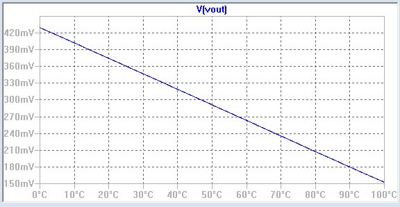
change of V by change of
T with 1uA of bias current
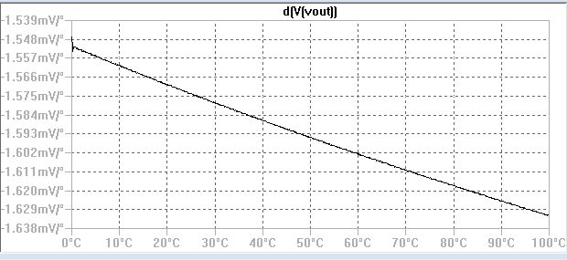
The change in voltage is about dV/dt = -1.6mV/C
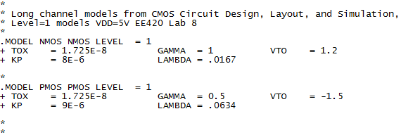
The characterization of PMOS and NMOS are on my lab 9 and below is its spice model
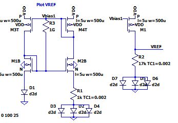
Now to get a band gap voltage reference in necessary to have the combination of
CTAT and PTAT. Ideally both slopes would cancel out, since CTAT is negative
slope and PTAT is positive of dV/dT.
One can choose the voltage reference value and then solve the necessary
components. However, we wanted to know how our circuit works based on the IC
that we had. So we solved for the components and then get Vref from them.
Similar to the process follow in pg.765 & 766 from the CMOS (course)
textbook.
The current mirror we constructed to bias the current we assumed that it would
drive enough current to maintain all of the transistors in saturation based on
our experience of experiment LAB 9.
Considerations
We wanted to provide a current mirror with 30uA
Vref of about 1.2 V
Use p-n diodes to build the PTAT and CTAT
Use a big resistor to start-up the circuit.
Use of K=3 diodes
Operation
Calculations
But, we observed that the experiment result was more similar with
the general diode model provided in the CMOS textbook
L = (dV/dT)/(n*Ln(K)*0.085)
with n=1 for silicone and K=3
L = 17
Diode parameters
Is= 1e-18 n =1
Choosing Iref = 30u
R= n*VT*Ln.(K)/Iref =952 --> 1k
Iref = (Vd1-Vd2)/R --> n*VT*Ln.(K)/R1
Vd = n*VT*Ln.(Iref/Is) =0.776 V
Vd2 = n*VT*Ln.(Iref/(K*Is)=0.75
Vd3
= Vd2
Vref= Vd3+Iref*L*R1 = 1.26V
Vref = 1.26V
dVd/dT
= 1.6mV/`C
dVT/dT=
0.085mV/`C
dVref/dT= d(N*VT*Ln(K)*L)/dT +dVd/dT
dVref/dT=1*0.085m*ln(2)*17)-1.6)
= 0 V
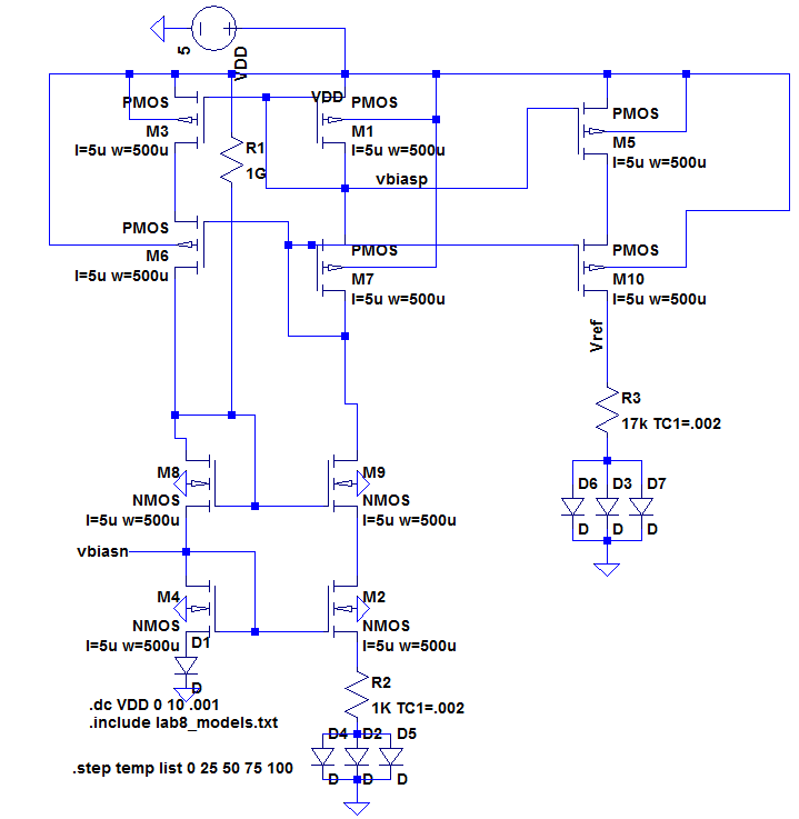
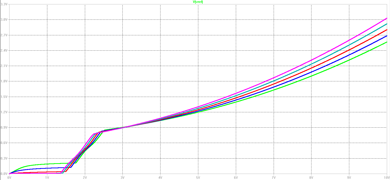
Experiment Results:
|
|
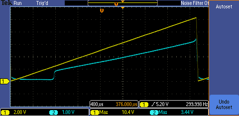
Under
normal conditions The
experiment shows that the operating VDD is 2.25 V. And
gives a Vref of .9 V and then goes up to 3.2 V for VDD = 10. Which
very close to the simulated values (operating VDD=2.25 V à Vref= .8 V and VDD=10V à3V |
|
|
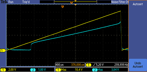
Here
is a sample of what happened when heat is add to the CTAT part of the circuit,
VDD
operating point for this circuit goes to 2 |
|
|
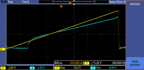
Here
is a sample of what happened when heat is added to PTAT of the circuit. The
output (Vref) increases Here
the VDD operating voltage is about 1.6 a lot lower than the original BGR
measurement. |
|
|
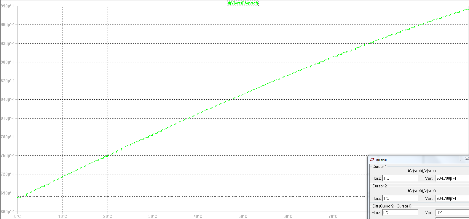
Since
we wanted to get a TCV of 0 we simulated the TCV=(1/Vref)(dVref/dT). We couldn’t do the
experiment but since the simulation and experiment is very similar, I
conclude that the simulation is reliable. TCV
we got for 23`C is 765uV/`C |
Conclusion
In this lab we learned of another way to have a voltage reference besides the
Beta multiplier. However, in this experiment (and simulations) we saw that the
Vref does change as VDD changes. On the other hand, we also saw how having a
bang gap reference circuit give fewer changes in voltage caused by temperature.
The adding of an amplifier would give a better Vref; it would be more VDD
independent. Also, if more `transistors are add to make the current mirror in cascode
form we could get a better VDD independence.
For different process we get similar results.
With Cascode for example we got the following result: