EE 420L Engineering Electronics II Lab - Project
Nha Tran
04/23/2015
NSHE: 2000590233
trann4@unlv.nevada.edu
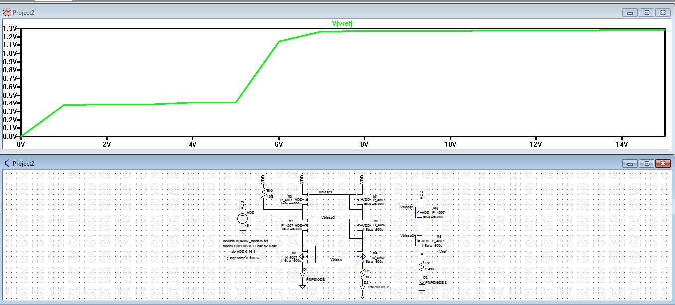
Project - using
as many diodes, resistors, and capacitors as needed, along with two
CD4007 chips from the same production lot (see date code on the top of
chip) to ensure current mirrors are possible, design and build a
bandgap voltage reference (BGR). Your report, in html, should detail
your design considerations, simulation results (using the models you
generated in lab 8), and measured results showing the BGR's performance (how the reference voltage changes with VDD). It would be good, but it's not required, if you could also characterize the BGR performance with temperature.
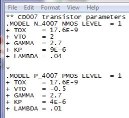
The
project did not specify how much current we can draw from the circuit
so we just pick R=1k for simplicity. Next we choose K=8, which is the
value of the diode multiplier again this is just for preference since
we know that ln 8 = 2. this will make calculation easier for us. From
equation 23.31; R=1k, ln K = 2, n = 1, Vt = 0.026 for room temperature,
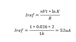
plugging
in all the known values we got Iref = 52uA. In our simulation we got
Iref=46.6uA. The calculated value and simulation is close.
Using
equation 23.35 since we dont want our Vref to change with temperature
we set dVref/dT = 0 and solve for L. we can estimate the change in
diode voltage with temperature dVd/dT = -1.6mV/C. This estimation is
taken from figure 23.20 in the book.
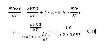
now
we use the equation 23.34 in the book to find Vref. With all the values
known we got Vref=1.19V. so our simulation should be close to this
value and will not change with changing VDD.
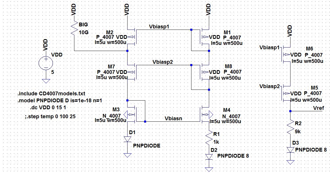
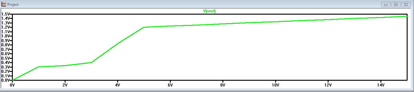
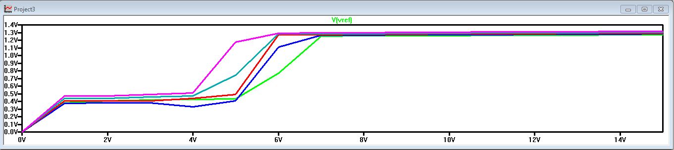
This
design was not our first choice. at first we choose the topology with
both the Pmos and Nmos cascoded. but that didnt do so well for us. So
we were adviced to change to this topology. from the graph below you
can see that Vref changes slightly with VDD but not much, the change
could be because our spice model of the transistor does not match the
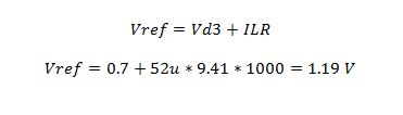
actual chip. the spice model for lab8 and 9 that we used are below
Below is the spice model file that i found online
of the CD4007 chip, this model is also a level one model, but has all
the other parameter. I used it to simulate the same topology as above
to see the difference in the model files in created using experiment
and the one that is created by the company who manufactured the chip,
as you can see vref is more stable but it seems the mosfet doesnt turn
on until ~6V.
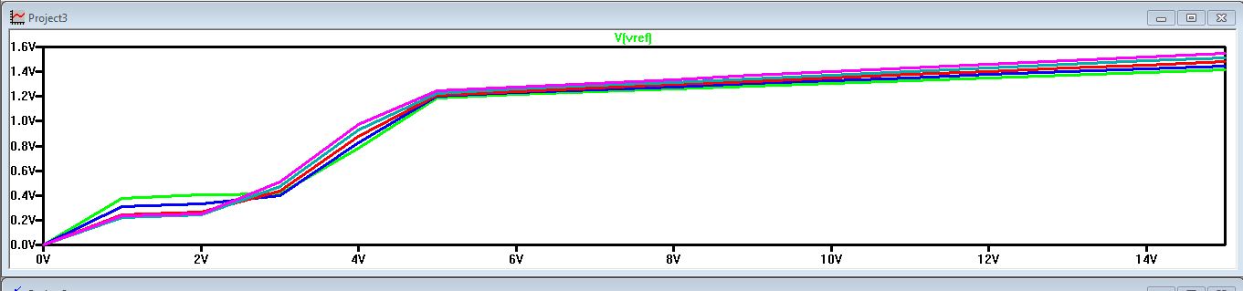
Below
is a sweep of temperature from 0-100 with 25 degree increment to see
how the BGR changes with temperature. the first plot is of the models
we created and the second plot is the model we pulled online. The model
we created changes slightly with VDD while the one we pulled online
does not change with VDD.
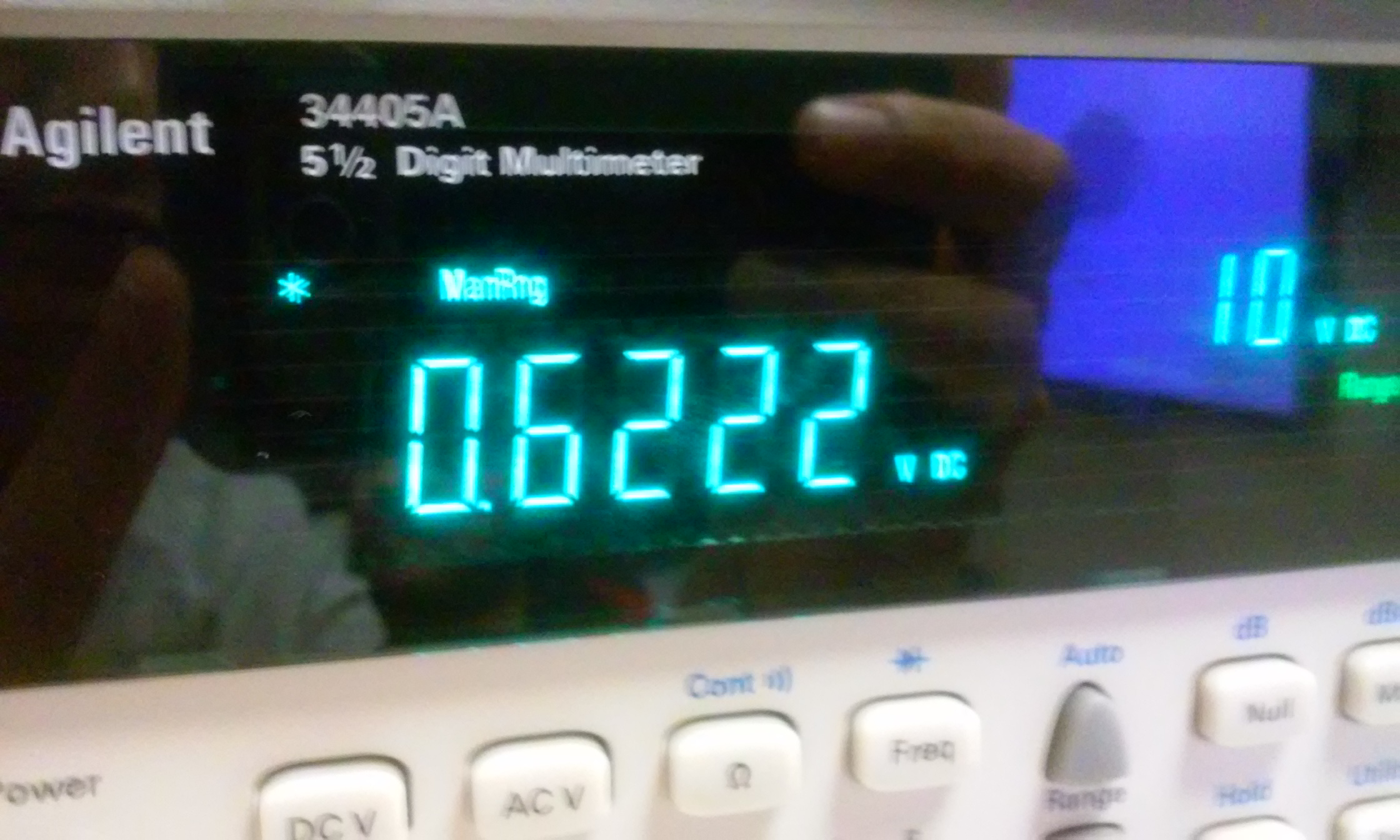
Experimentally
we was not able to get our transistor to turn on using 2 cascoded nmos
and pmos, we had Vref= 0.62V at 5V vdd which doesnt seen right because
in our simulation we had Vref at ~1.2V at around 3V vdd. We took data
for 2 cascode BGR from 5V to 15V vdd. below is the images that we took
in lab. We was gonna use this data as our lab report but luckily we
found dr. Baker and he advised us to only use the pmos cascoded and we
was able to get the desired result. As you can see below Vref does stay
constant at ~1.3 when VDD > 6V.
Experiment
of our design in lab. as you can see we tried many different diode.
because at first we didnt know why our simulation show the right values
but the experiment did not. We thought it was the diode models because
in lab we could not find the same diode model that we used for
simulation. 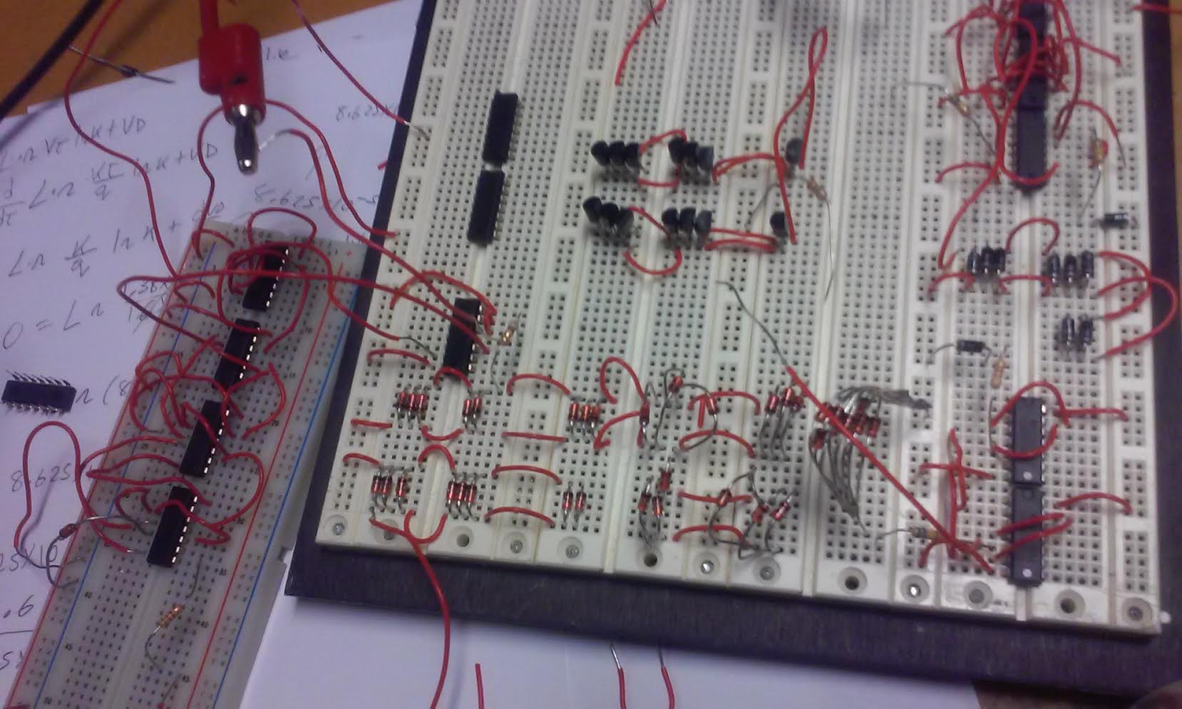
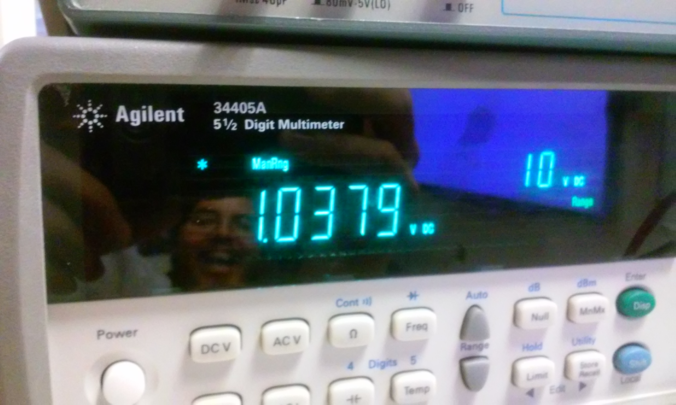
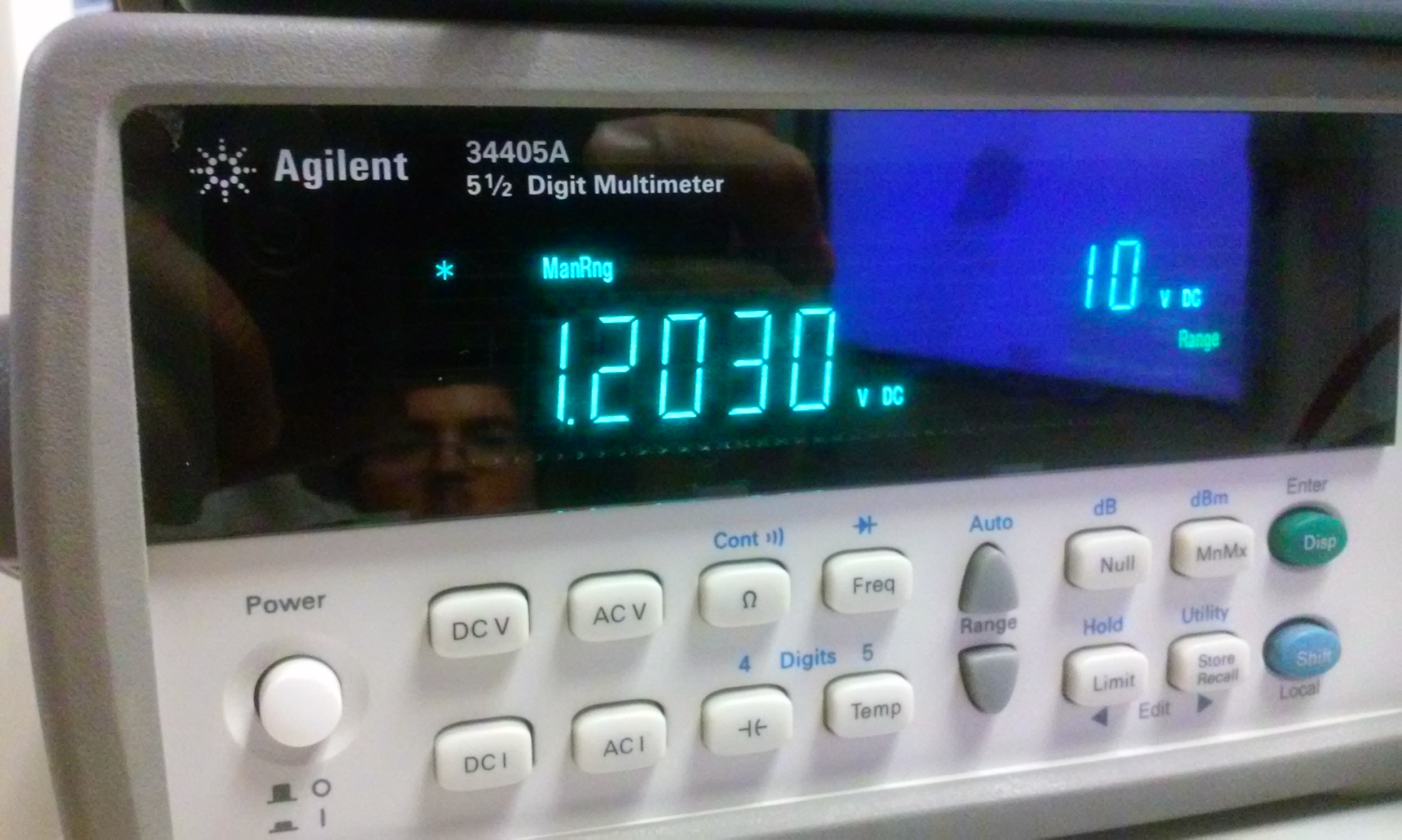
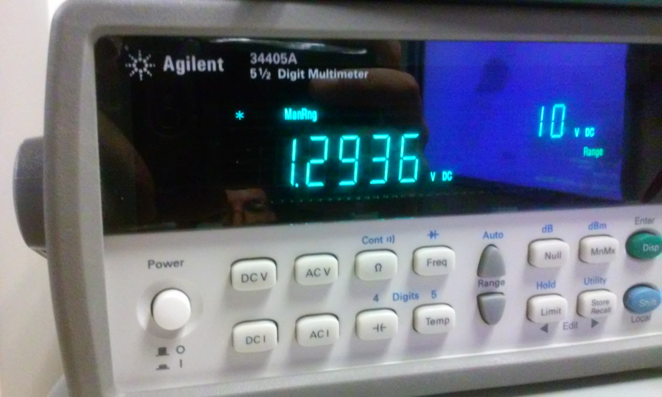
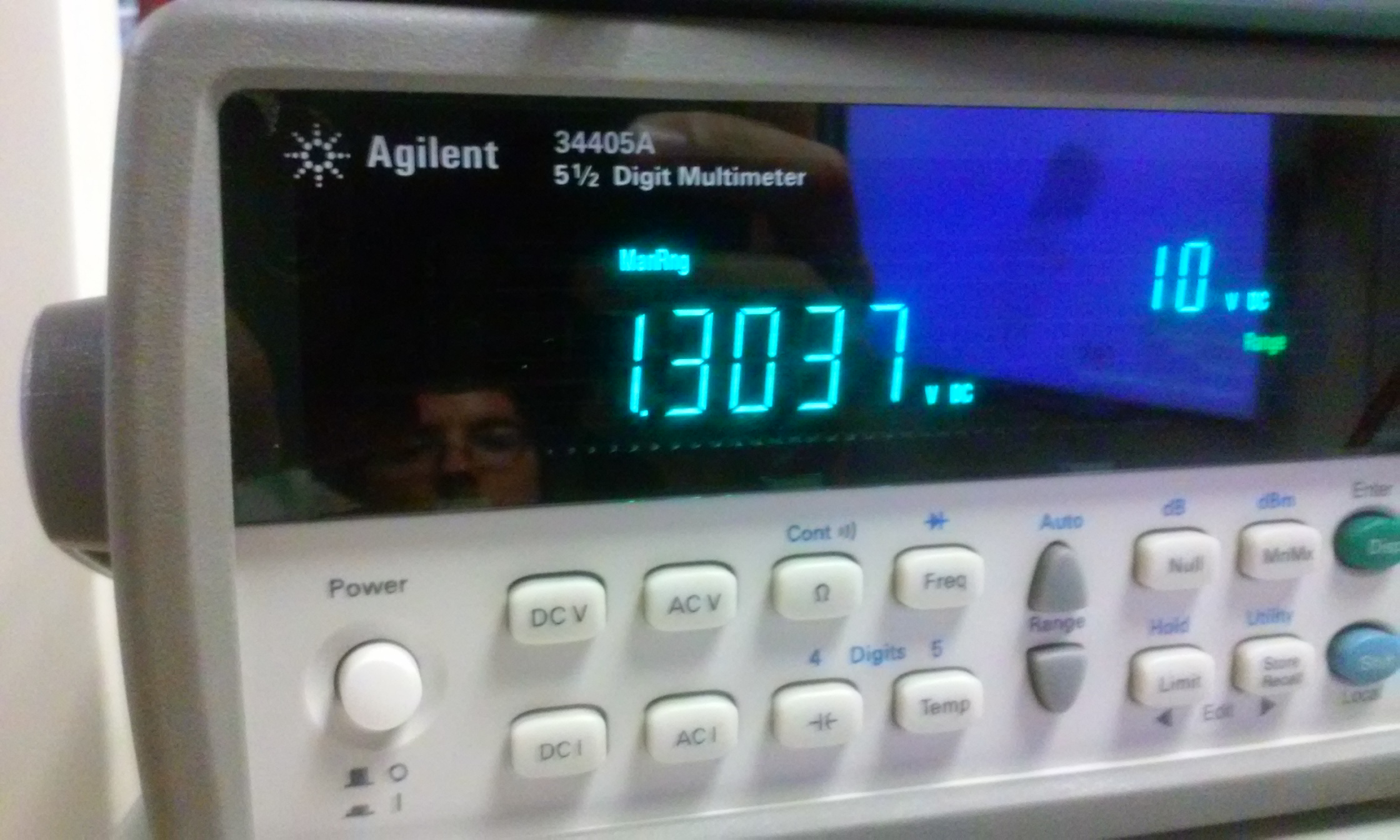
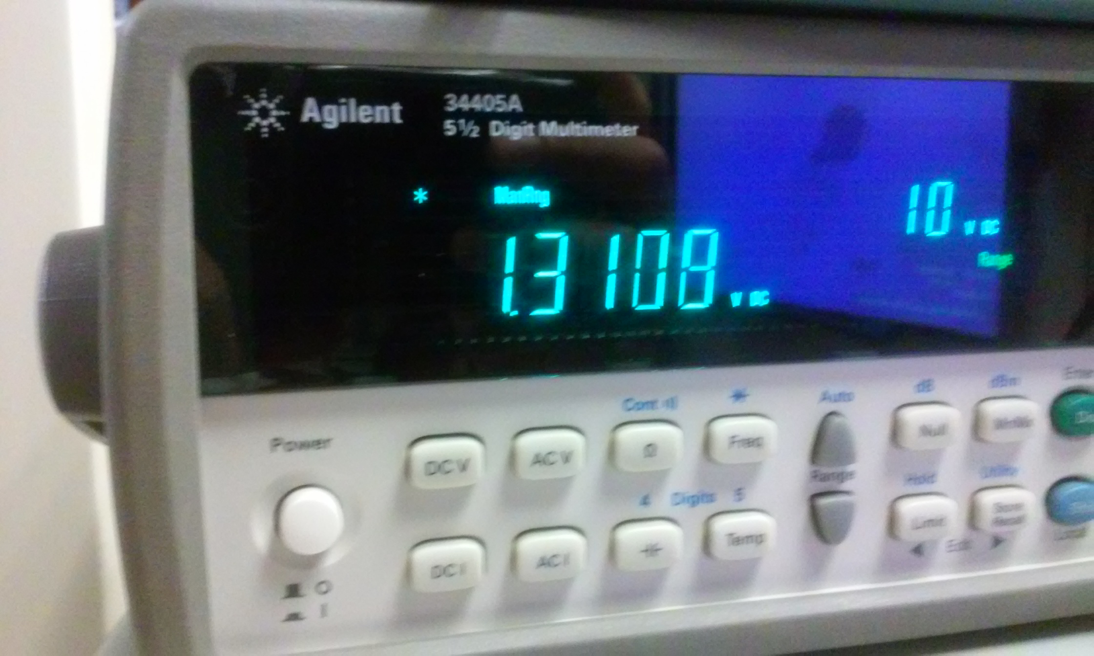
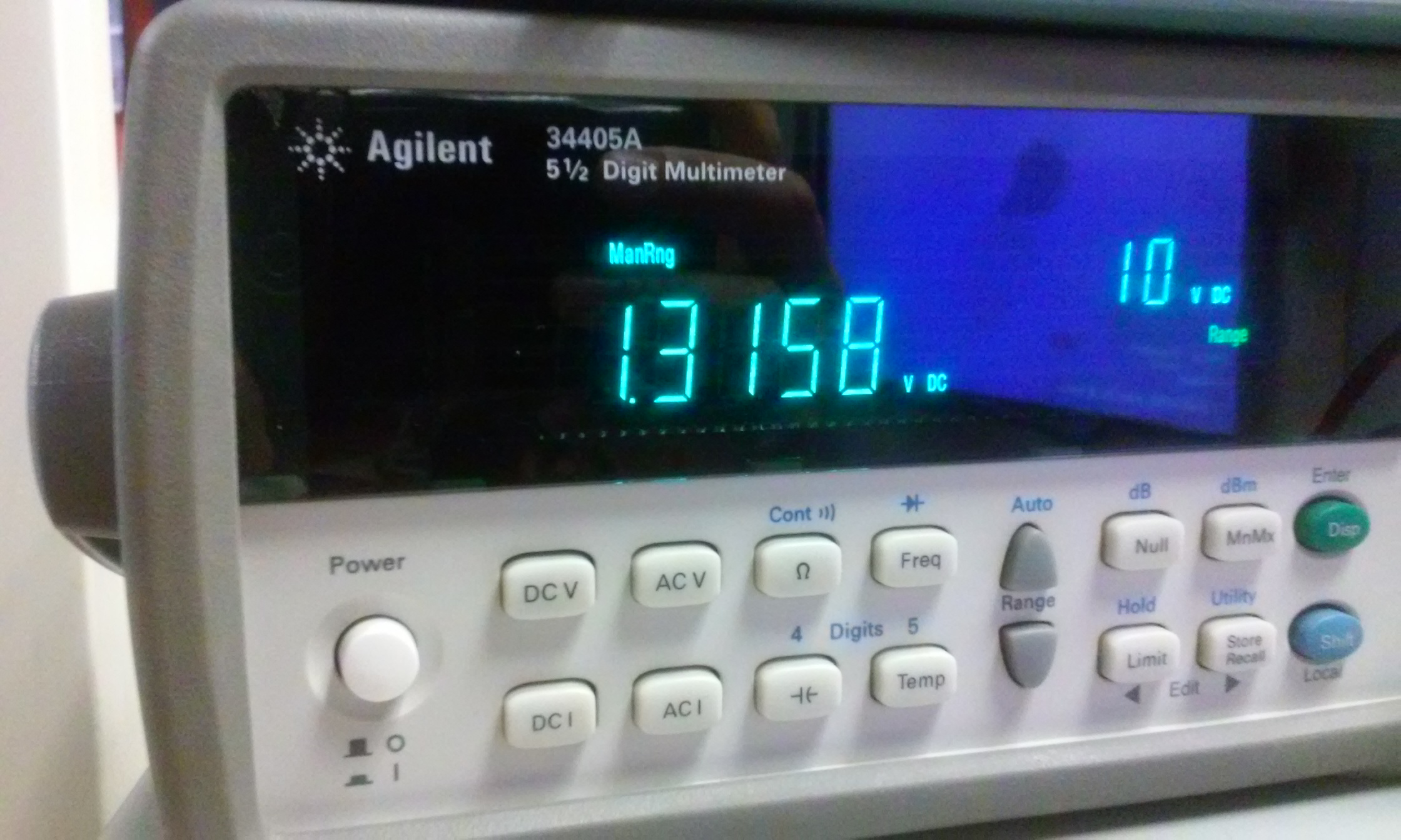
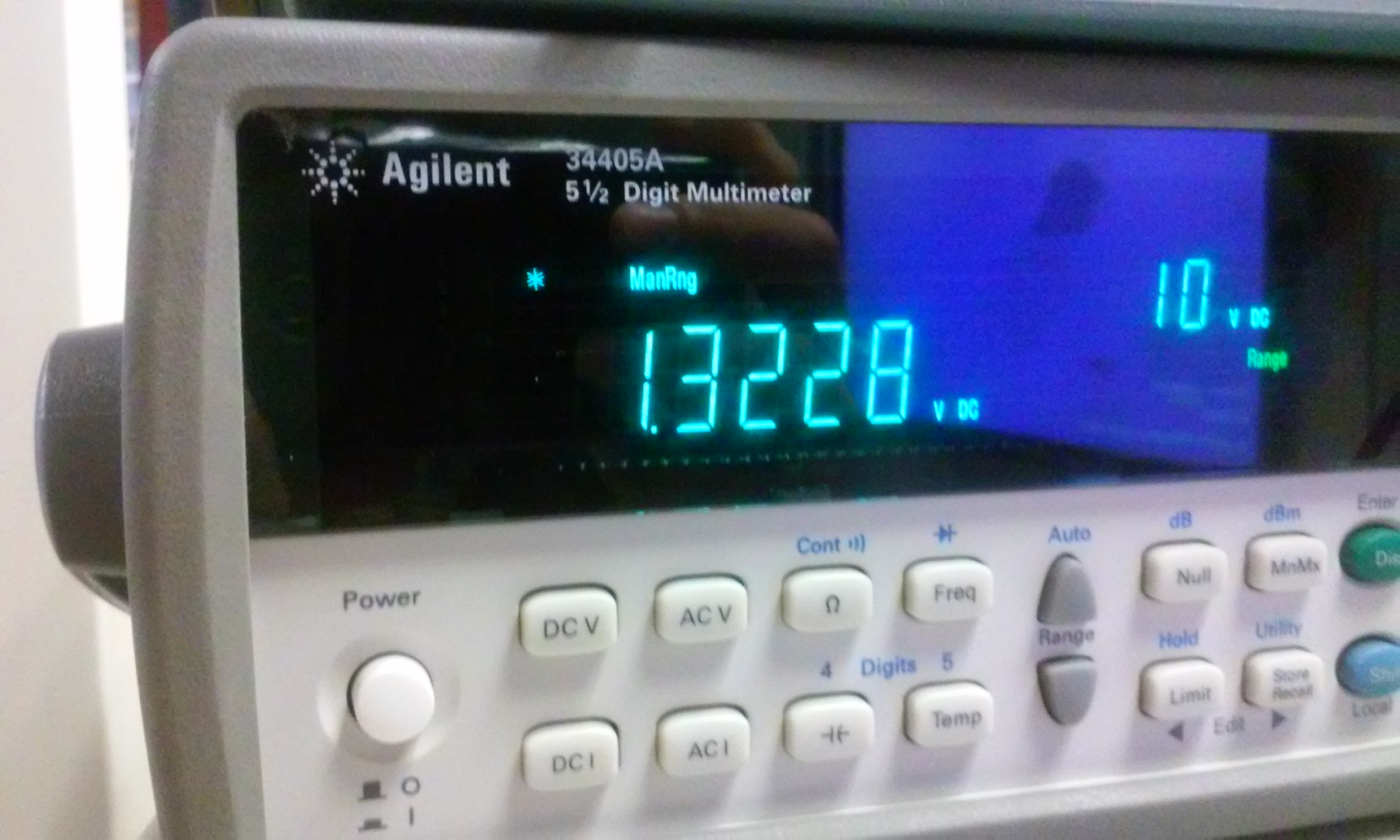
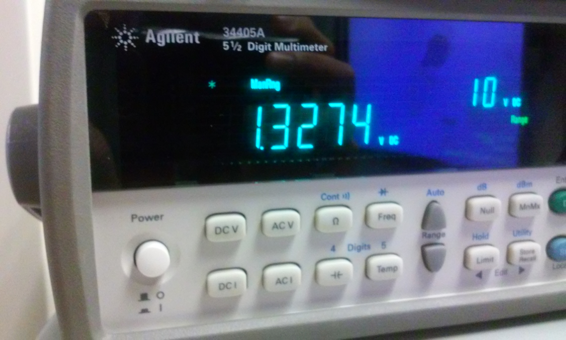
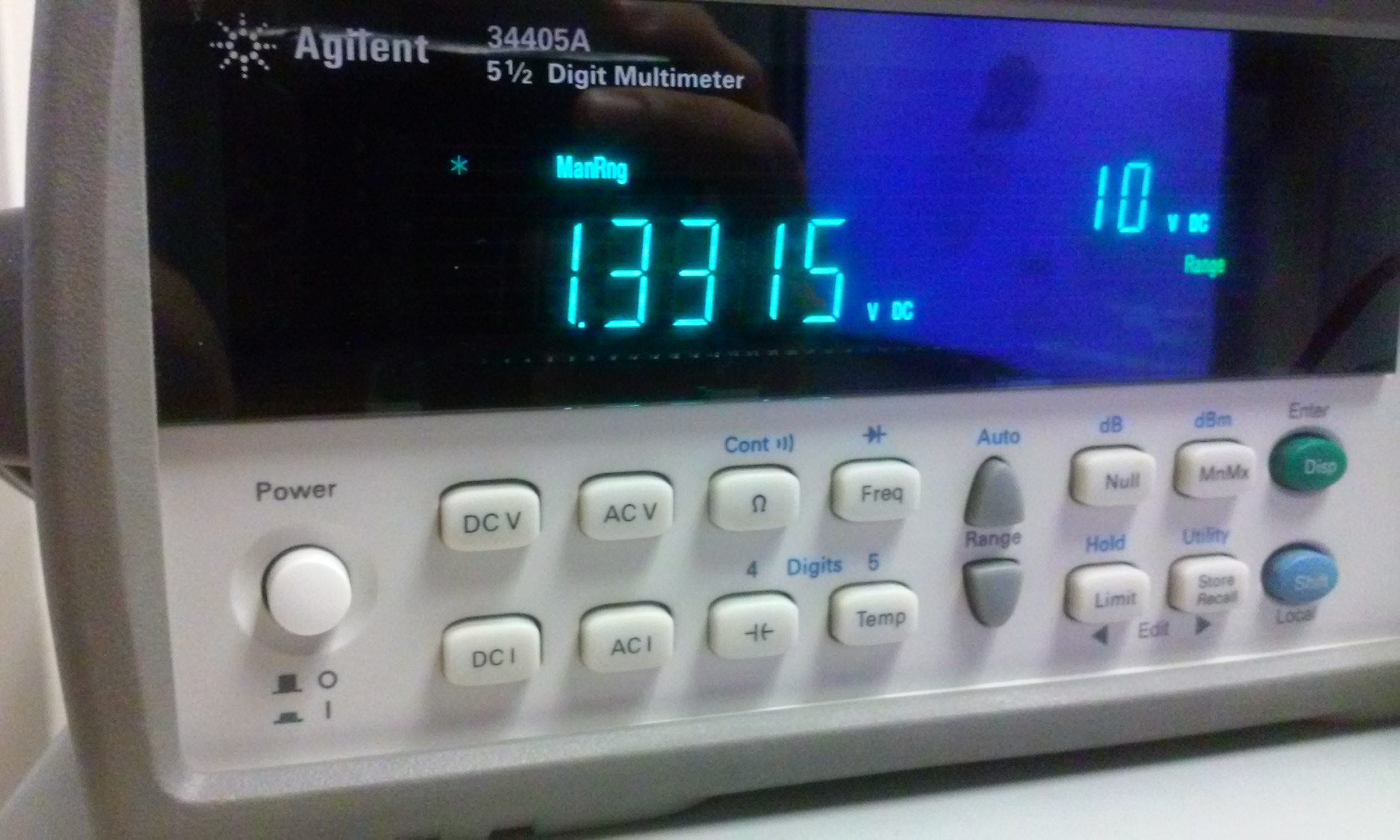
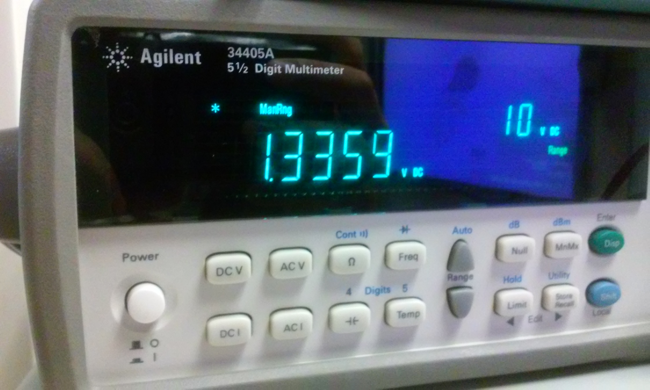
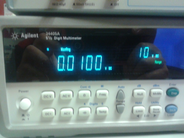
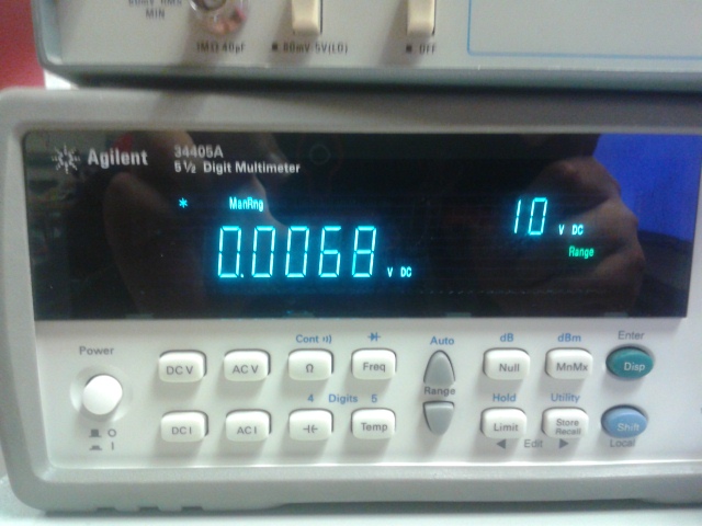
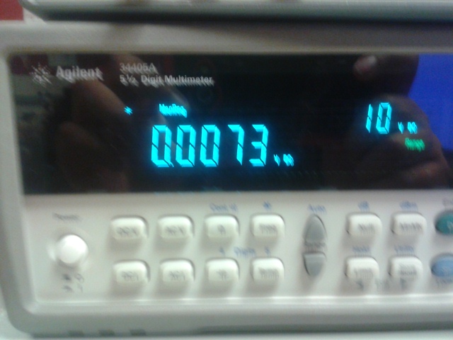
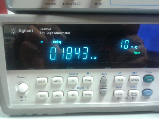
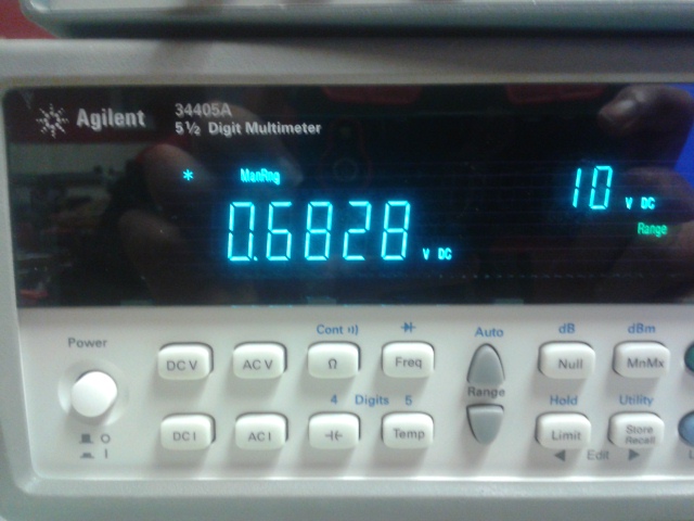
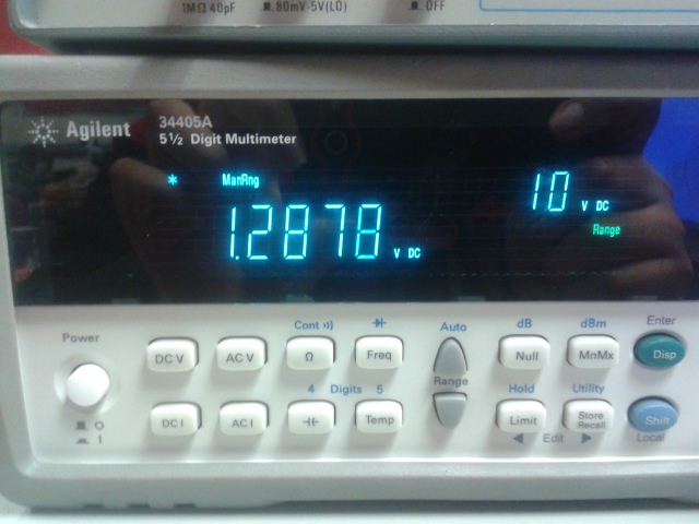
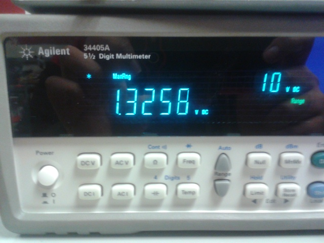
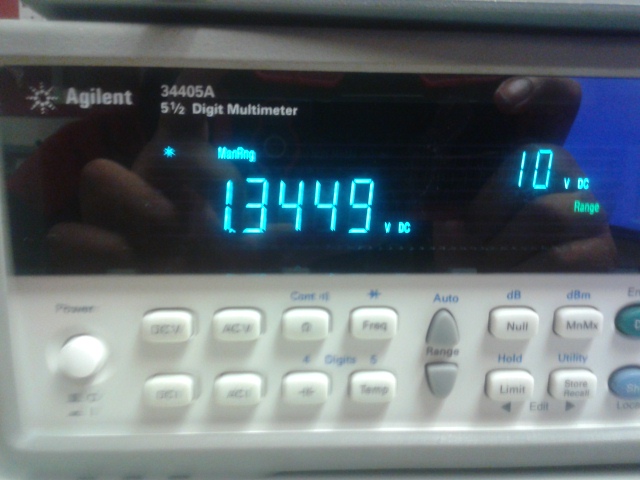
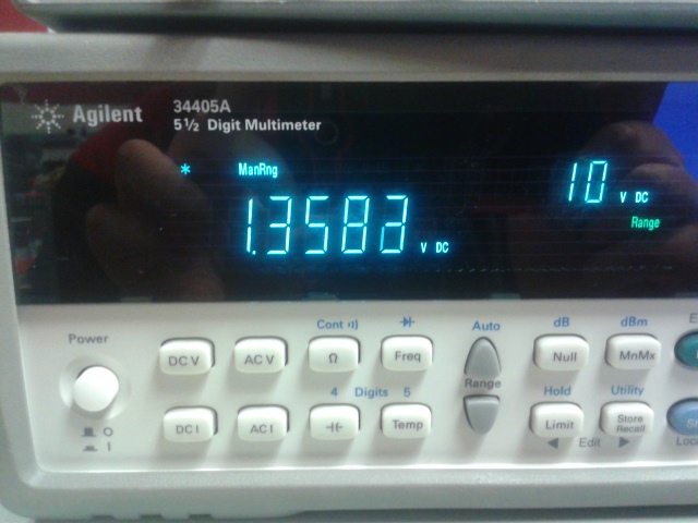
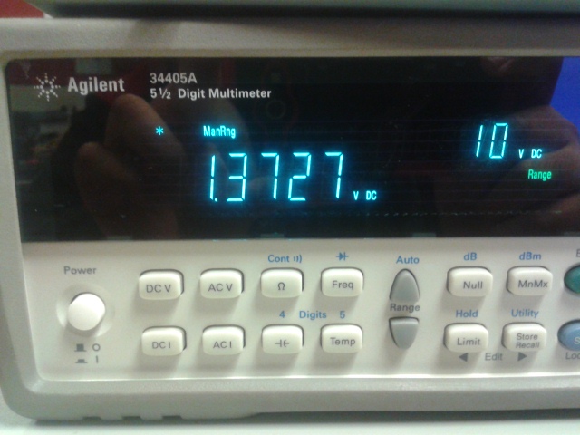
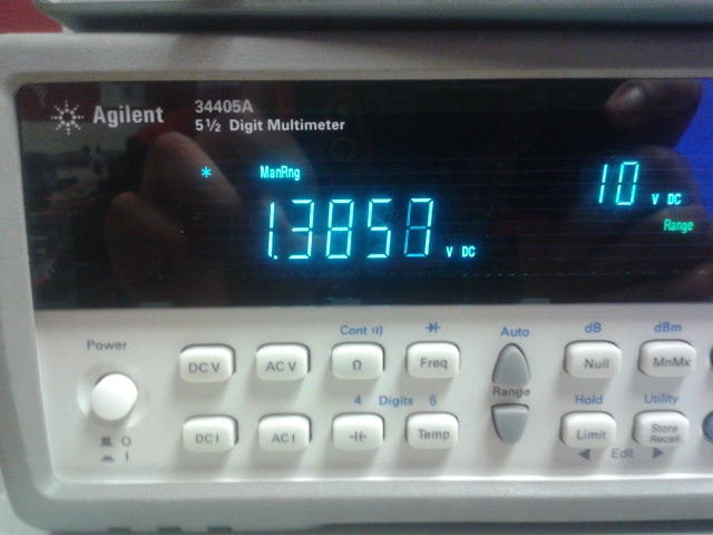
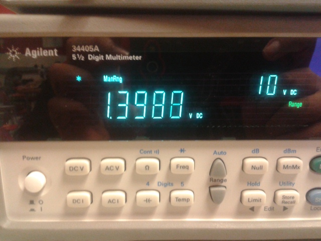
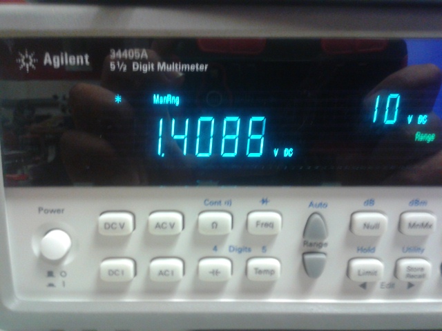
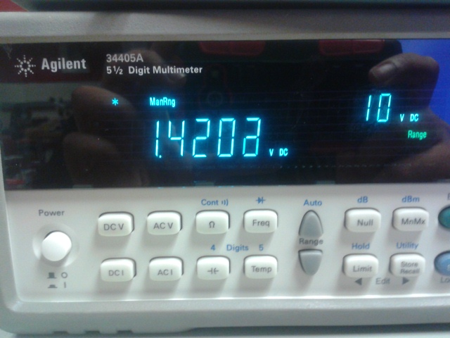
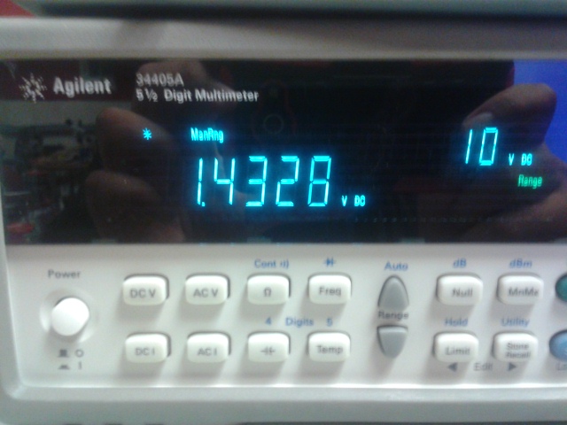
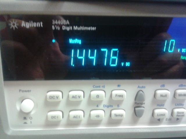
Below we measured Vref using a multimeter, we vary VDD from 0V to 15V. each picture below correspond to increment of VDD.
Using
the data we took in lab, then we plot Vref vs VDD in excel to show that
Vref does not vary greatly with vdd. As you can see from the graph when
VDD is greater than 5V, Vref remain relatively constant.

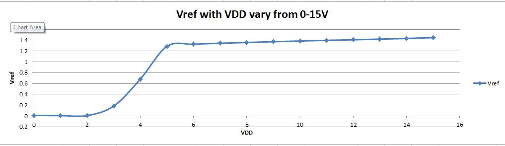
Conclusion:
This is the first time that our simulation gave us a worst result than
our experiment. This is because our model that we created for the
CD4007 did not match the chip that we were using. the numbers could be
close that is why we had variation when we measure Vref. In our
experiment we ran into alot of troubles while trying to measure Vref.
But once we got it to work the result is better than our simulations.
In our simulation Vref changes from 1.2V to 1.42V when VDD varies from
5 to 15V, an change of 220mV. In our experiment Vref changes from
1.2878V to 1.4476V when Vdd varies from 5V to 15V. The experimental and
simulation Vref is very close but the experiment is better.
Return to EE420L front page