EE 420L Engineering Electronics II Lab - Lab 9
Nha Tran
04/23/2015
NSHE: 2000590233
trann4@unlv.nevada.edu
Design of a Beta-Multiplier Reference (BMR) using the CD4007 CMOS transistor array
Pre-lab work
- This lab will use the level=1 MOSFET model created in lab 8 and, again, the MOSFETs in the CD4007.pdf CMOS transistor array.
- Design and simulate the operation of a BMR that biases the NMOS devices so that they have a gm of 20 uA/V
- Use a simple (big) resistor to VDD for the start-up circuit (explain how the addition of a resistor ensures start-up).
- When
the BMR is operating the current in the big resistor should be much
smaller than the current flowing in each branch of the BMR
- Write-up,
similar to a homework assignment, your design calculations and
simulation results. (This will count as the pre-lab quiz.)
- Ensure that you show the following in what you turn in:
- Hand calculations
- Operation as VDD is swept from 0 to 10 V
- Vbiasn
should stabilize (be constant) after VDD hits a minimum value (estimate
this value of VDD assuming VGS/VSG is a threshold voltage and
VDS,sat/VSD,sat is zero).
- Vbiasp should follow VDD after VDD hits a minimum value (show this in simulations)
- Unstable operation if too much capacitance is shunting the BMR's resistor (see bottom of page 630)
- Comments comparing the hand calculations with the simulation results
In this lab you may need to use two,
or more, CD4007 chips from the same production lot (see date code on
the top of chip) to ensure using a BMR to bias a current mirror is
possible. If the CD4007 chips are not from the same production lot they
will not "match" so current mirrors will not be possible.
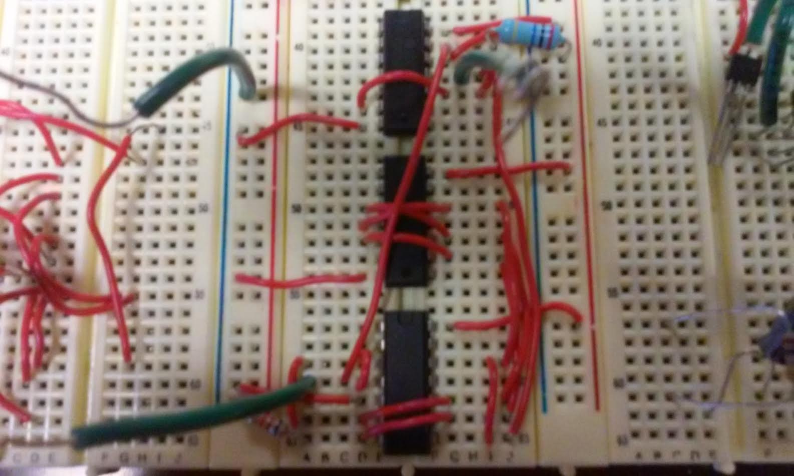
- Build your BMR design and characterize it as you did in the pre-lab
- You
expect the BMR to become unstable if there is a large capacitance
across the resistor, such as a scope probe (important), so care must be
exercised
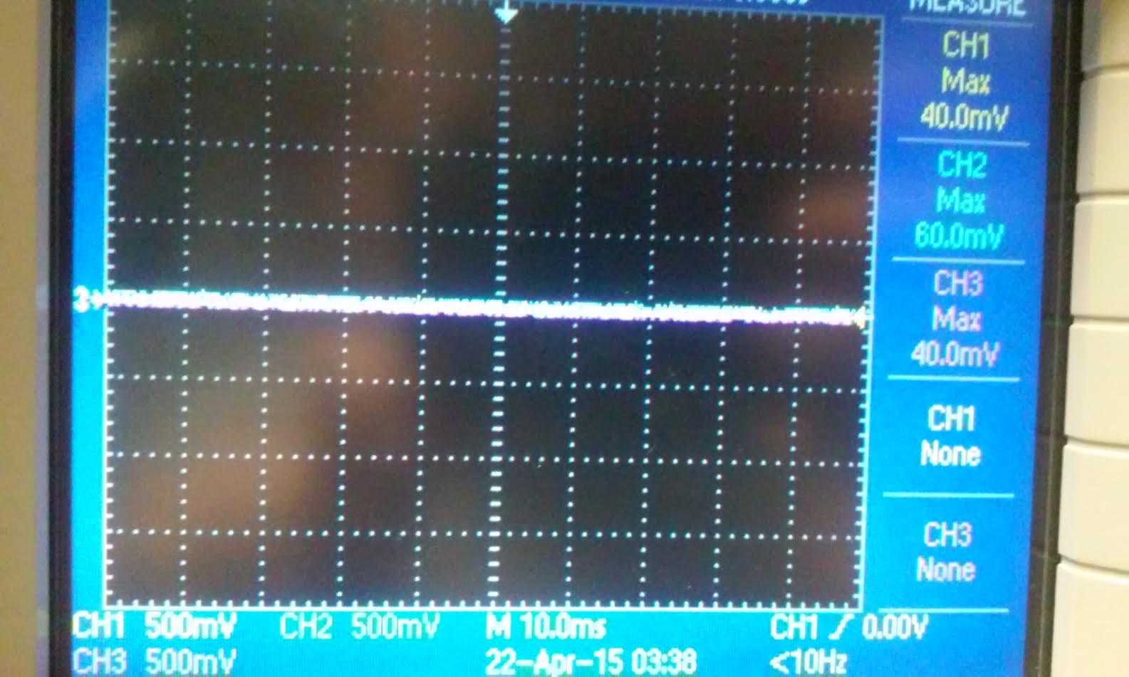
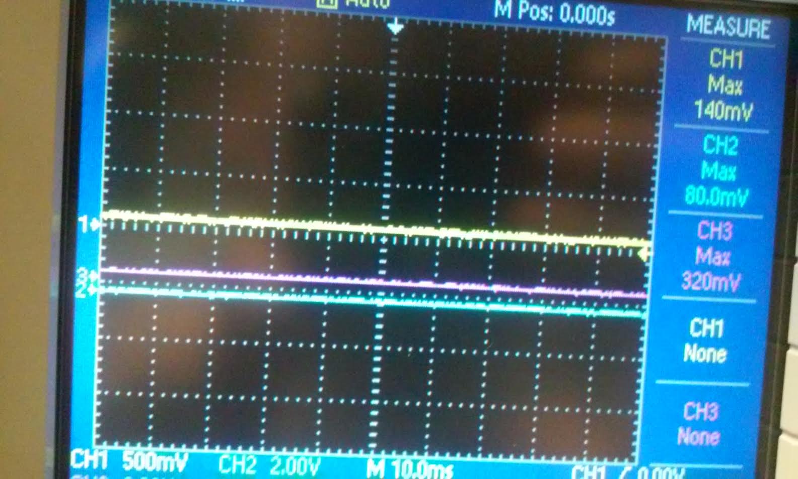
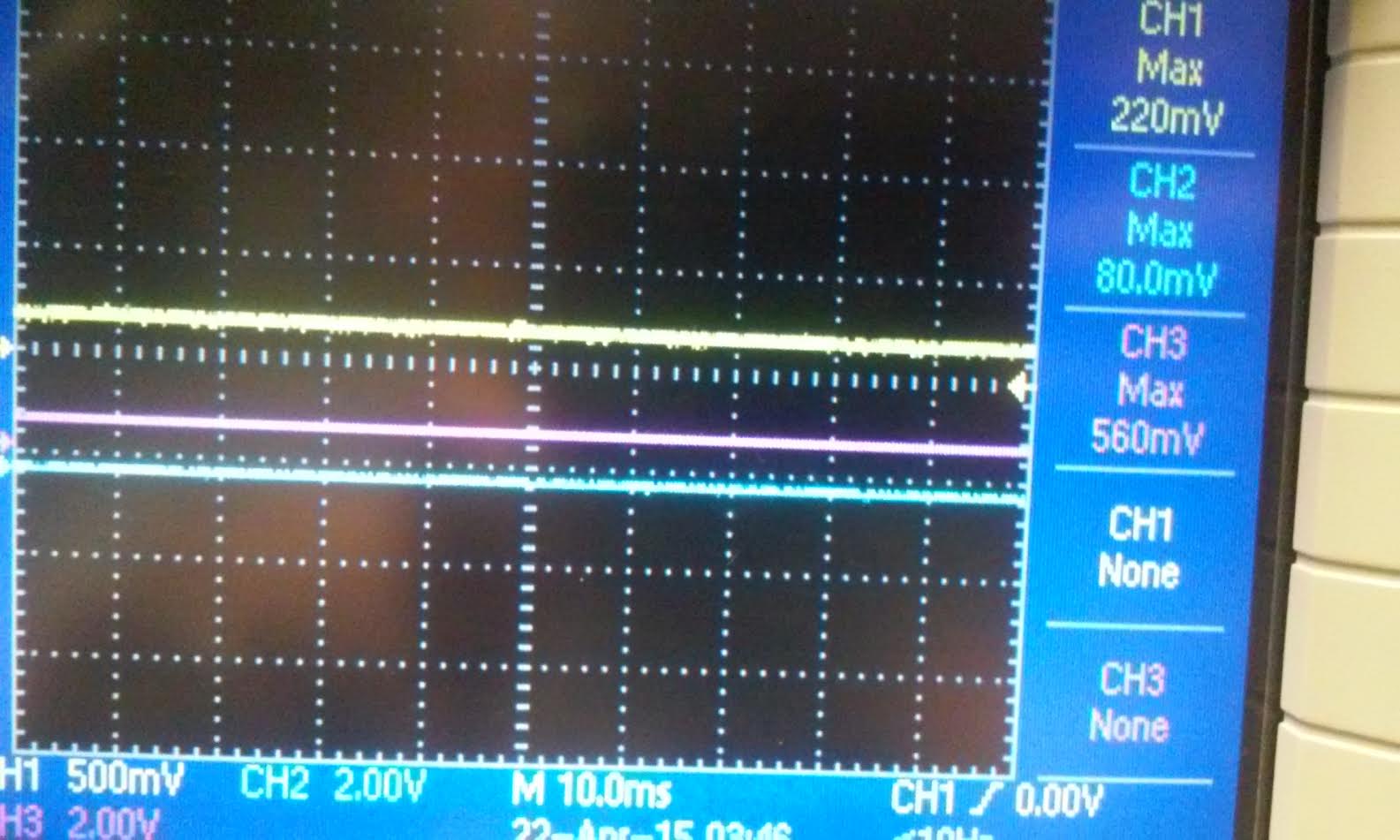
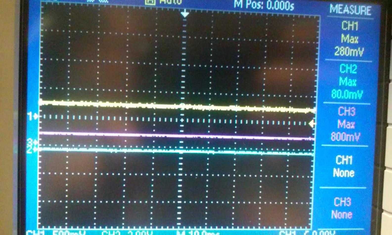
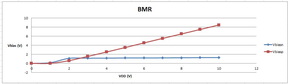
In Lab we took individual points
of Vbiasn and Vbiasp using the oscilloscope and plot them using excel.
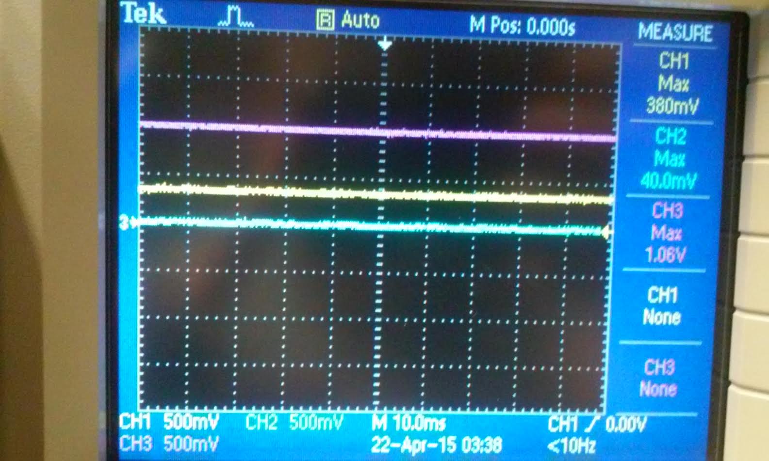
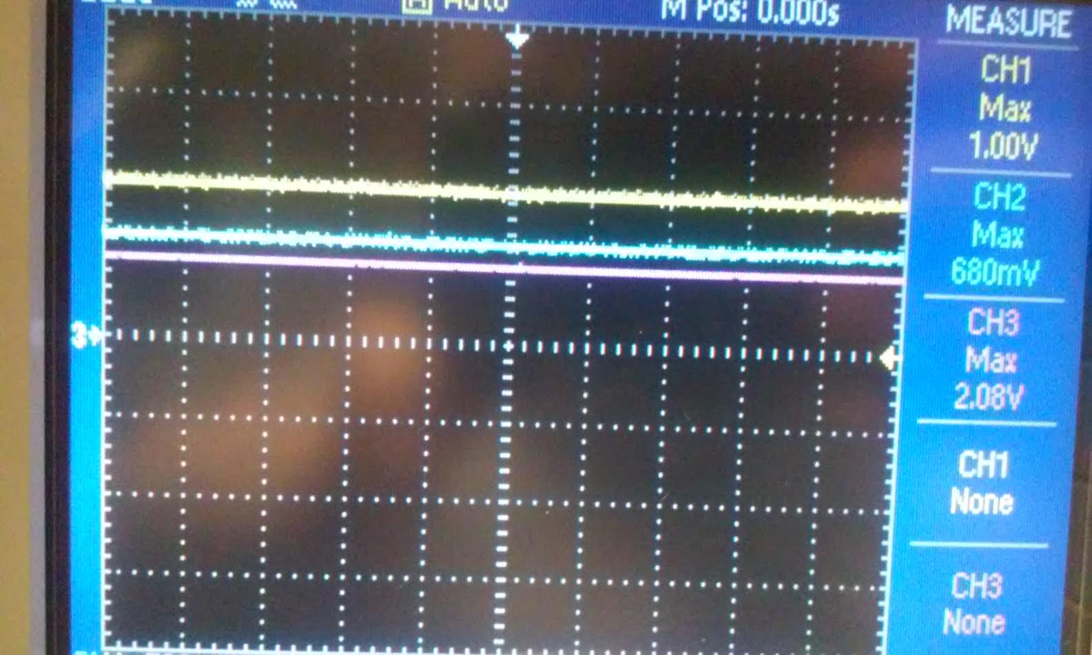
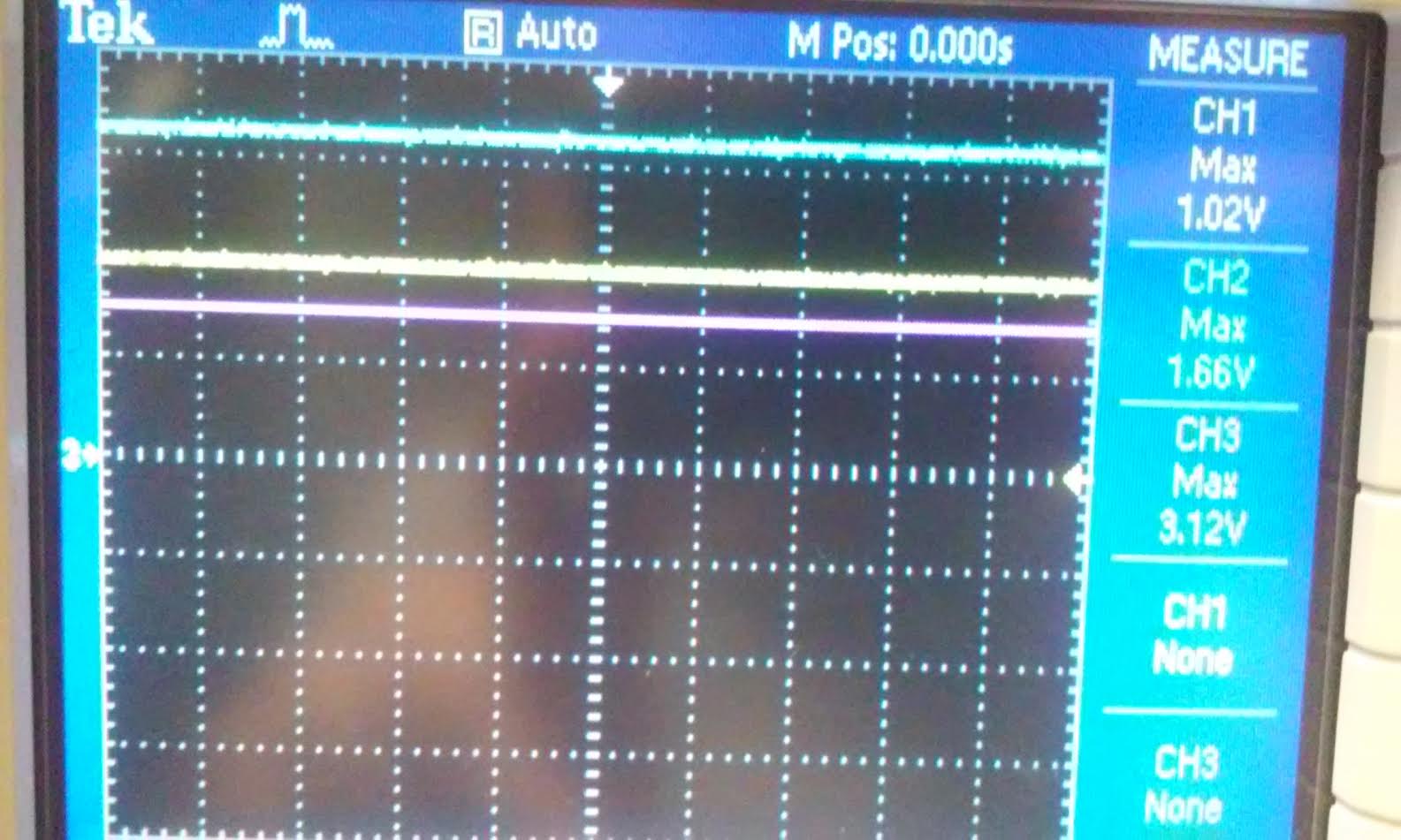
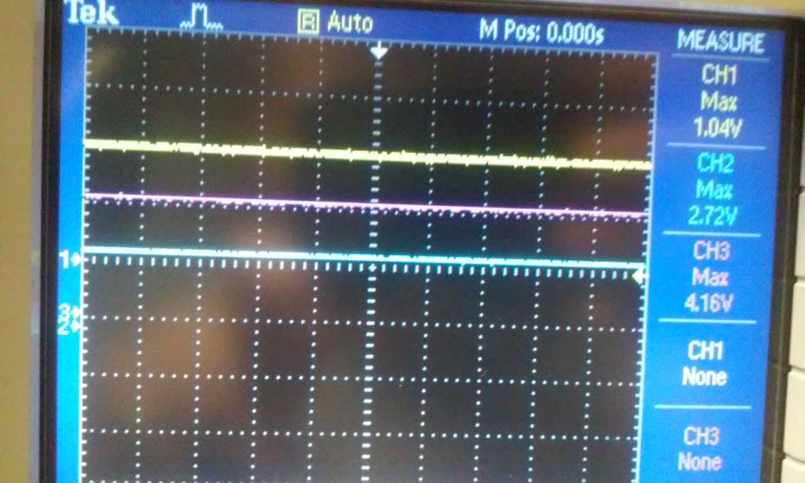
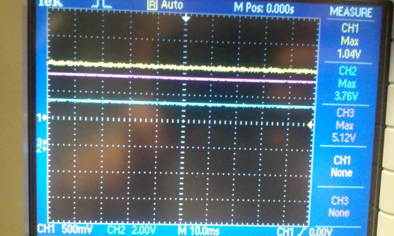
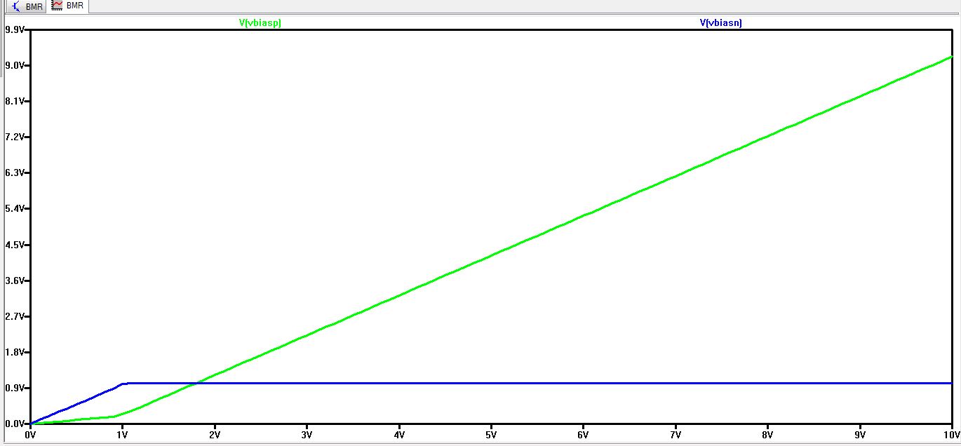
Below is image of Vbiasn and Vbiasp along with our circuit, channel 3
(purple scope) is vdd, we varied VDD from 0 to 10V. as you can see from
the scope as VDD approaches 2V Vbiasn (channel 1, yellow) becomes
stable at ~1V and stays at 1V when VDD >2V. Vbiasp (Channel 2, blue)
continues to increase with increasing VDD. We only took picture up to
when VDD=5V after awhile you can see the trend.
Data taken from oscope reading: use to plot vbiasn and vbiasp using excel| VDD | 0 | 1 | 2 | 3 | 4 | 5 | 6 | 7 | 8 | 9 | 10 |
| Vbiasn | 0.0008 | 0.154 | 1.11 | 1.14 | 1.16 | 1.19 | 1.19 | 1.21 | 1.24 | 1.27 | 1.99 |
| Vbiasp | 0.004 | 0.003 | 0.61 | 1.53 | 2.5 | 3.49 | 4.5 | 5.5 | 6.47 | 7.46 | 8.44 |
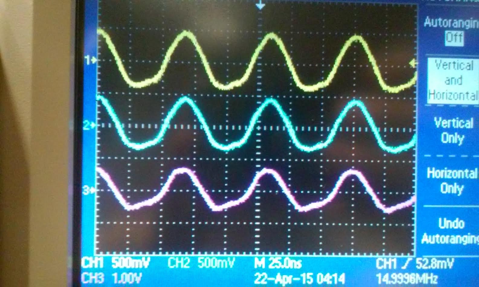
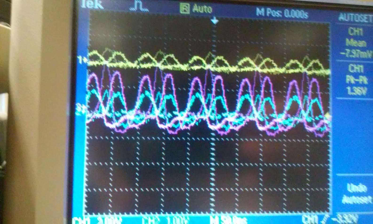
| Stable circuit no big capacitor added | Unstable with a big cap added (8.2uF) |
 |  |
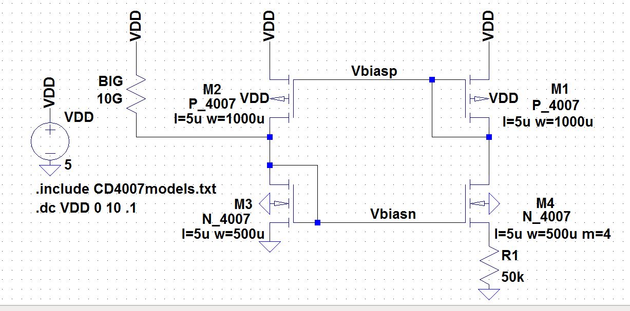
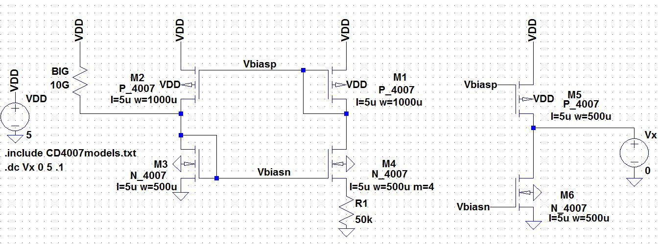
LTSpice simulation and schematic of BMR design which we used to do our experiment with.
. - Use your BMR to bias, and thus create, a:
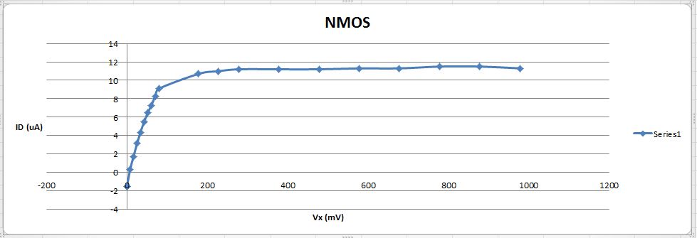
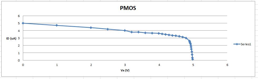
| VXvs | 0 | 0.01 | 0.02 | 0.03 | 0.04 | 0.05 | 0.06 | 0.07 | 0.08 | 0.09 | 0.1 | 0.2 | 0.25 | 0.3 | 0.4 | 0.5 | 0.6 | 0.7 | 0.8 | 0.9 | 1 |
| Vx (mV) | 0.4 | 0.4 | 8.05 | 16.29 | 25.5 | 33.74 | 42.9 | 52.15 | 61.1 | 70.8 | 80 | 178 | 228 | 278.3 | 378.2 | 478 | 578 | 677.8 | 777.8 | 877.8 | 977.6 |
| ID (uA) | -1.5 | -1.5 | 0.3 | 1.7 | 3.15 | 4.36 | 5.5 | 6.5 | 7.3 | 8.3 | 9.1 | 10.7 | 11 | 11.2 | 11.2 | 11.2 | 11.3 | 11.3 | 11.5 | 11.5 | 11.3 |
| VXvs | 5 | 4.99 | 4.98 | 4.97 | 4.96 | 4.95 | 4.94 | 4.93 | 4.92 | 4.91 | 4.9 | 4.8 | 4.7 | 4.6 | 4.5 |
| Vx (V) | 4.988 | 4.9793 | 4.9695 | 4.9602 | 4.9498 | 4.9402 | 4.9298 | 4.9205 | 4.9105 | 4.9009 | 4.8908 | 4.7905 | 4.6907 | 4.5917 | 4.492 |
| ID (uA) | 0.133 | 0.335 | 0.785 | 1.16 | 1.5 | 1.78 | 2.02 | 2.21 | 2.37 | 2.51 | 2.6 | 3 | 3.14 | 3.22 | 3.3 |
| | | | | | | | | | | | | | | |
| VXvs | 4.5 | 4.4 | 4.3 | 4.2 | 4.1 | 4.0 | 3.8 | 3.6 | 3.4 | 3.2 | 3 | 2.5 | 2 | 1 | 0 |
| Vx (V) | 4.491 | 4.391 | 4.2913 | 4.1917 | 4.0914 | 3.9914 | 3.1917 | 3.592 | 3.3921 | 3.1922 | 2.9924 | 2.4929 | 1.993 | 0.9936 | 0.0042 |
| ID (uA) | 3.3 | 3.36 | 3.42 | 3.5 | 3.55 | 3.63 | 3.67 | 3.7 | 3.8 | 3.8 | 4.0 | 4.2 | 4.4 | 4.7 | 5 |
schematic in LTspice and simulation of basic NMOS, PMOS current mirror.
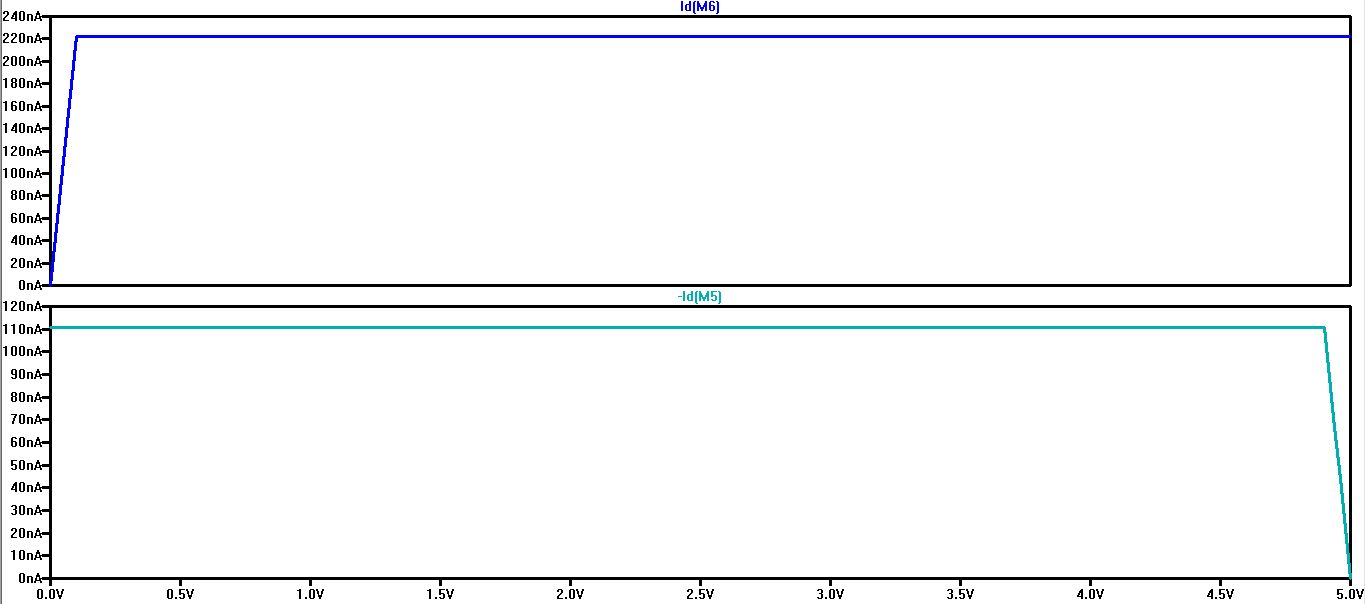
Measure how the current varies through each current mirror as the voltage across the mirror changes.- Of
course the current in the NMOS (PMOS) current mirror goes to zero as
the voltage on the drain of the output device moves towards ground (VDD)
experiment done above- Using these current mirrors drive two gate-drain connected transistors
- For the first experiment use the NMOS current mirror to drive two PMOS gate-drain connected devices.
- Use
the voltages on the gate-drain connection of the two devices to bias a
cascode current mirror (characterize this mirror as before)
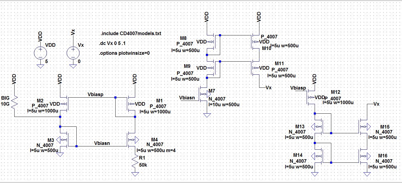
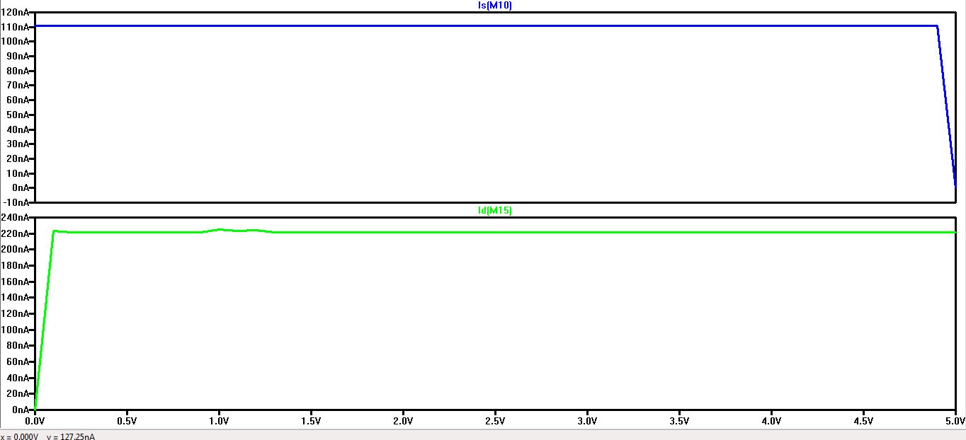
the
blue trace is the Nmos cascode current mirror and the green trace is
the Pmos cascode mirror. the experiment was done below using the above
schematic. the data was taken using the multimeter.
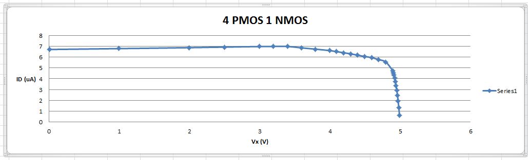
| 4 PMOS 1 Nmos Cascode |
| VXvs | 5 | 4.99 | 4.98 | 4.97 | 4.96 | 4.95 | 4.94 | 4.93 | 4.92 | 4.91 | 4.90 | 4.80 | 4.7 | 4.6 | 4.5 |
| Vx (V) | 4.9888 | 4.9793 | 4.9698 | 4.9602 | 4.951 | 4.9412 | 4.9319 | 4.9224 | 4.912 | 4.9025 | 4.8929 | 4.7932 | 4.6935 | 4.5942 | 4.494 |
| ID (uA) | 0.645 | 1.319 | 1.933 | 2.486 | 2.958 | 3.371 | 3.735 | 4.058 | 4.331 | 4.555 | 4.745 | 5.55 | 5.765 | 5.95 | 6.052 |
| | | | | | | | | | | | | | | |
| VXvs | 4.5 | 4.4 | 4.3 | 4.2 | 4.1 | 4.0 | 3.8 | 3.6 | 3.4 | 3.2 | 3.0 | 2.5 | 2 | 1 | 0 |
| Vx (V) | 4.494 | 4.394 | 4.2943 | 4.1944 | 4.0945 | 3.9947 | 3.795 | 3.5944 | 3.395 | 3.195 | 2.9952 | 2.4955 | 1.9958 | 0.9956 | 0.006 |
| ID (uA) | 6.052 | 6.175 | 6.3 | 6.4 | 6.5 | 6.6 | 6.73 | 6.85 | 6.98 | 6.98 | 6.97 | 6.92 | 6.87 | 6.78 | 6.7 |
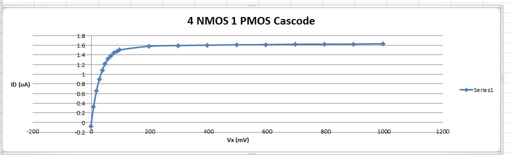
- For the second experiment switch, that is, use the PMOS current mirror to drive two NMOS gate-drain connected devices.
- Again, use these two voltages to bias an NMOS cascode current mirror then characterize.
| 4 NMOS 1 Pmos Cascode |
| VXvs | 0 | 0.01 | 0.02 | 0.03 | 0.04 | 0.05 | 0.06 | 0.07 | 0.08 | 0.09 | 0.1 | 0.2 | 0.3 | 0.4 | 0.5 | 0.6 | 0.7 | 0.8 | 0.9 | 1.0 |
| Vx (mV) | -1.4 | 8.05 | 17.94 | 27.5 | 37.5 | 47.16 | 57.3 | 67.05 | 77.25 | 87.05 | 96.75 | 196.8 | 296 | 396 | 496 | 596 | 696 | 796 | 896 | 996 |
| ID (uA) | -0.075 | 0.33 | 0.657 | 0.895 | 1.082 | 1.215 | 1.315 | 1.385 | 1.44 | 1.476 | 1.503 | 1.58 | 1.594 | 1.603 | 1.61 | 1.613 | 1.62 | 1.623 | 1.625 | 1.63 |
Return to EE420L front page