EE 420L Engineering Electronics II Lab - Lab 8
Nha Tran
03/15/2015
NSHE: 2000590233
trann4@unlv.nevada.edu
Pre-lab work
- Review the datasheet for the CD4007.pdf CMOS transistor array.
- Ensure
that you understand how the bodies of the NMOS are tied to pin 7 (VSS,
generally the lowest potential in the circuit, say ground) and that the
bodies of the PMOS are tied to pin 14 (VDD, generally the highest
potential in the circuit, say + 5V).
In
this lab you will characterize the transistors in the CD4007 and
generate SPICE Level=1 models. Assume that the MOSFETs will be used in
the design of circuits powered by a single +5 V power supply. In other
words, don't characterize the devices at higher than +5 V voltages or
lower than ground potential.
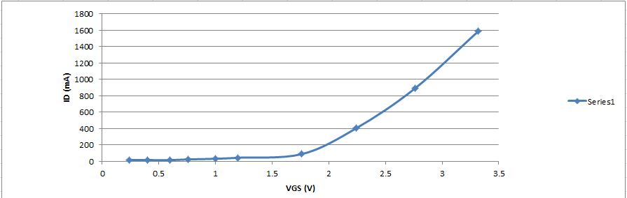
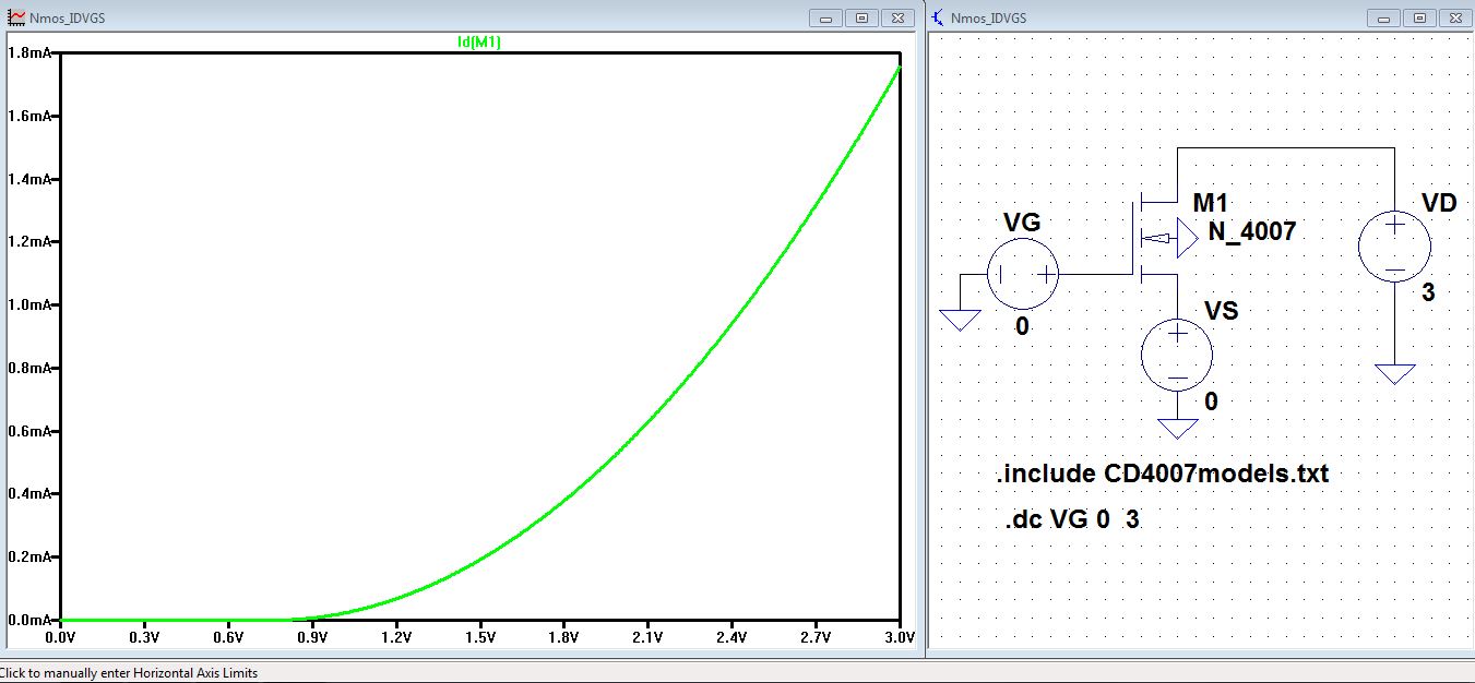
- Experimentally generate, for the NMOS device, plots of:
- ID v. VGS (0 < VGS < 3 V) with VDS = 3 V
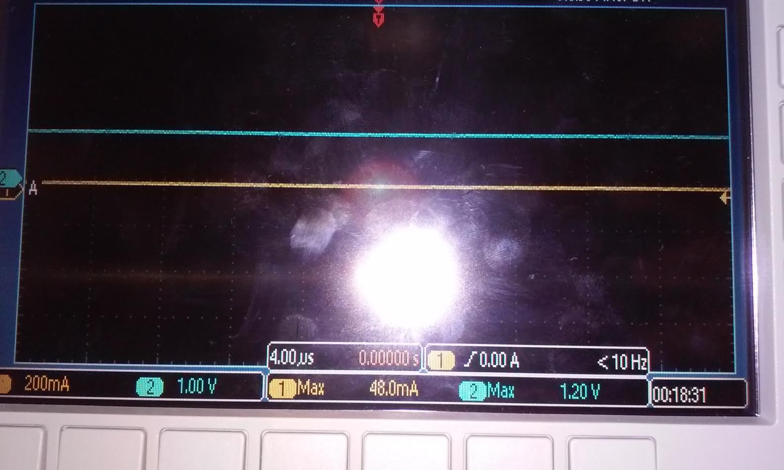
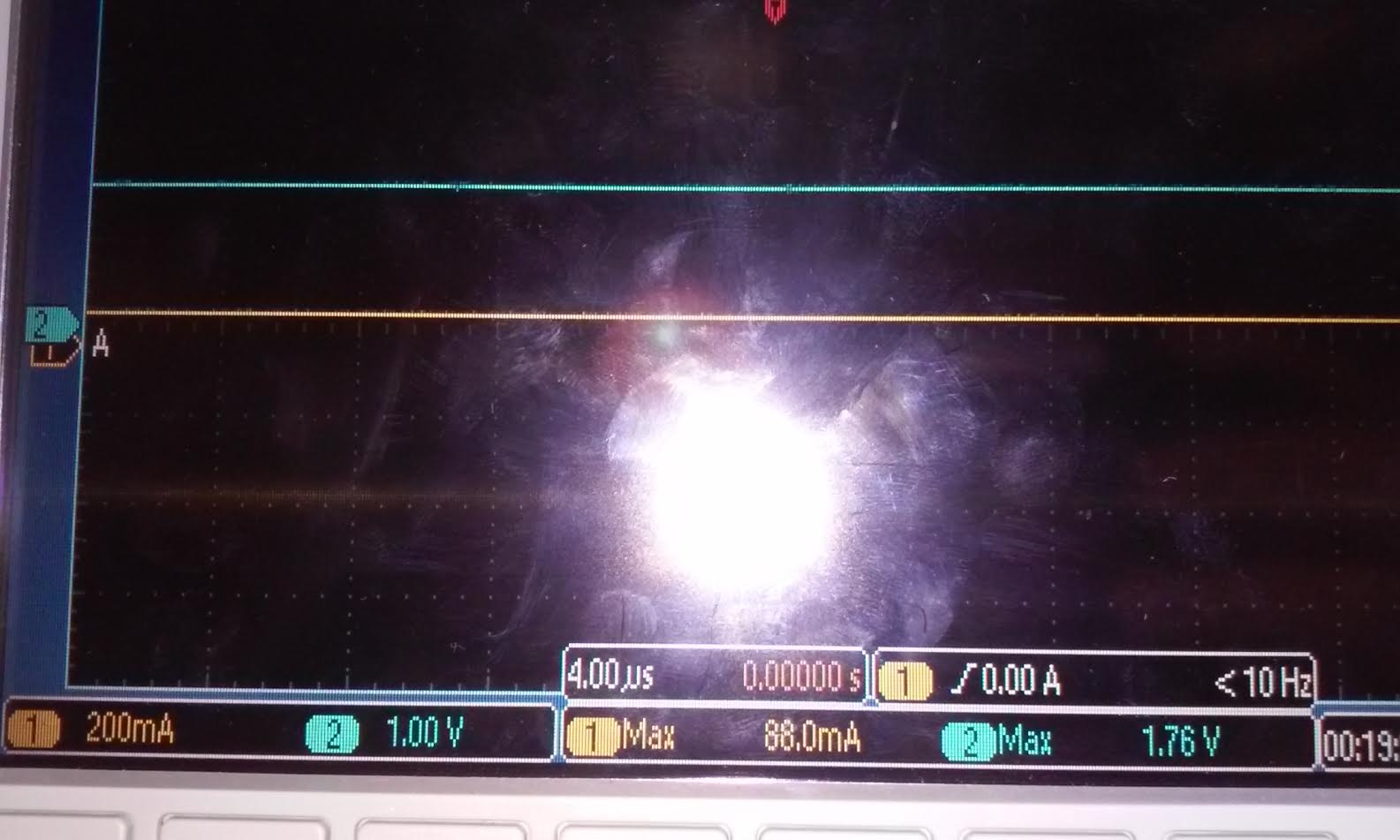
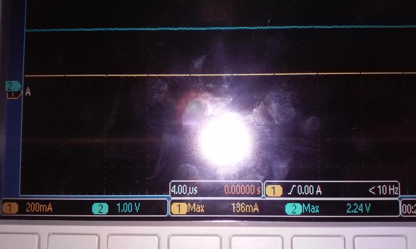
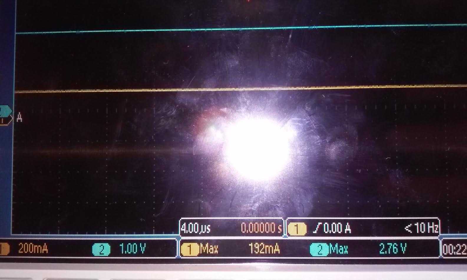
| ID (mA) | 16 | 16 | 16 | 24 | 32 | 44 | 88 | 403 | 890 | 1589 |
| VGS (V) | 0.24 | 0.4 | 0.6 | 0.76 | 1 | 1.2 | 1.76 | 2.24 | 2.76 | 3.32 |
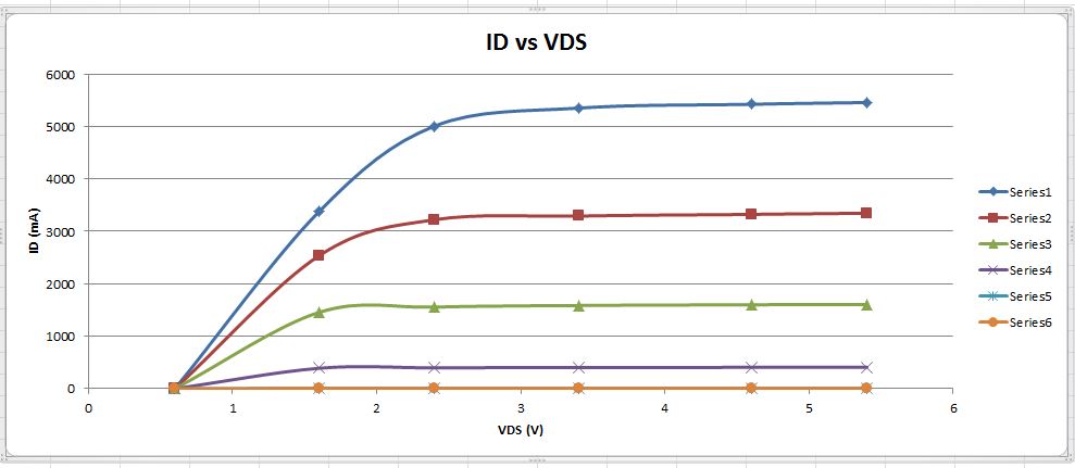
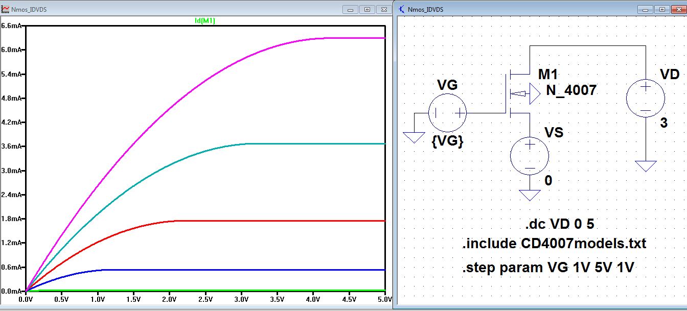
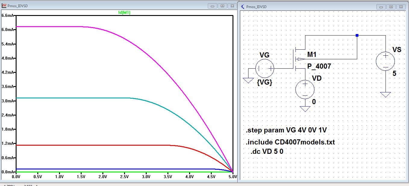
- ID v. VDS (0 < VDS < 5 V) for VGS varying from 1 to 5 V in 1 V steps, and
| VDS (V) | 0.6 | 1.6 | 2.4 | 3.4 | 4.6 | 5.4 |
| ID5 (mA) | 1.5 | 3378 | 5007 | 5352 | 5424 | 5458 |
| ID4 (mA) | 1.5 | 2536 | 3223 | 3292 | 3325 | 3347 |
| ID3 (mA) | 0.5 | 1456 | 1566 | 1587 | 1601 | 1602 |
| ID2 (mA) | 0.5 | 390 | 398 | 403 | 406 | 410 |
| ID1 (mA) | 0.3 | 3.6 | 3.7 | 4.3 | 5.2 | 5.5 |
| ID0 (mA) | 0.2 | 2.2 | 2.5 | 3 | 4 | 4.4 |
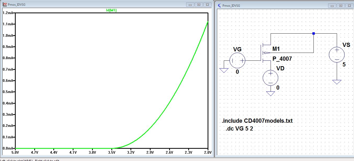
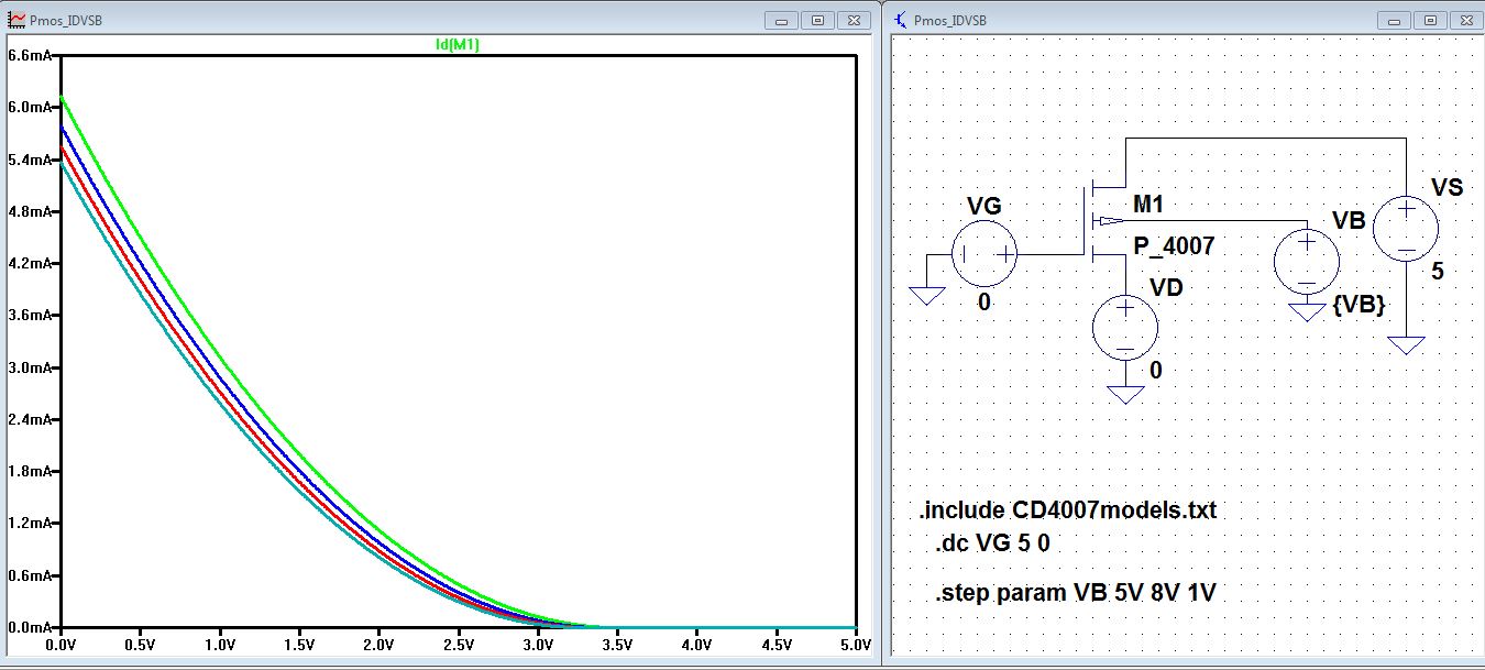
- ID v. VGS (0 < VGS < 5 V) with VDS = 5 V for VSB varying from 0 to 3 V in 1 V steps.
| VGS (V) | 0.6 | 1.6 | 2.4 | 3.6 | 4.4 | 5.2 |
| ID3 (mA) | 0 | 0 | 0 | 0 | 88 | 1821 |
| ID2 (mA) | 0 | 0 | 0 | 9.1 | 886 | 2580 |
| ID1 (mA) | 4.5 | 4.5 | 7.4 | 231 | 1946 | 3427 |
| ID0 (mA) | 3 | 4.2 | 400 | 1603 | 3348 | 5462 |
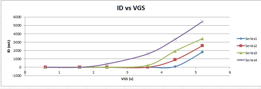
- Note
that for this last one, if VSS (NMOS body) is ground (again, the
Body, VB, is grounded) then the source voltage will be varied from 0 to
3 V in 1 V steps to realize VSB ( = VS - VB = VS) varying from 0 to 3 V
in 1 V steps. At the same time VGS will be varied from 0 to 3 V (when
VS = 0), 1 to 4 V (when VS = 1 V), 2 to 5 V (when VS = 2 V), and 3
to 5 V (when VS = 3 V). In other words, as VS is increased by 1 V the
VGS has to shift up by 1 V as well.
- Assuming
that the length of the NMOS is 5 um and its width is 500
um calculate the oxide thickness if Cox (= C'ox*W*L) = 5 pF.
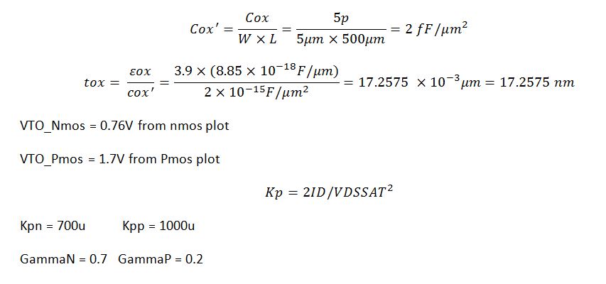
- From this measured data create a Level = 1 MOSFET model with (only) parameters: VTO, GAMMA, KP, and TOX.
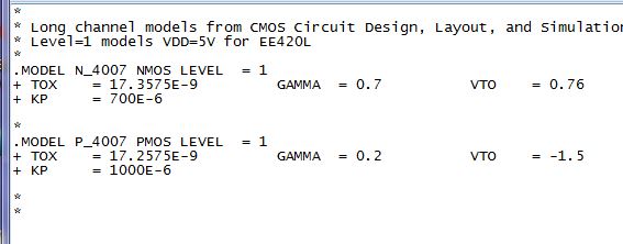
here is the link to the 4007 text model - Compare
the experimentally measured data above (the 3 plots) to
LTspice-generated data (again, 3 plots) and adjust your model
accordingly to get better matching.
ID vs VGS, VDS = 3V; 0<VGS<3V
ID vs VDS; VGS varies from 1V-5V; 0<VDS<5V
ID vs VGS; VDS=5V; VBS varies from 0-3V; 0<VGS<5V
- Repeat the above steps for the PMOS device where VDS, VGS, and VSB are replaced with VSD, VSG, and VBS respectively.
ID v. VSG (0 < VSG < 3 V) with VSD = 3 V | VGS | 0 | 1 | 2 | 3 |
| ID | 15.9 | 15.8 | 127.6 | 869.7 |
ID v. VSD (0 < VSD < 5 V) for VSG varying from 1 to 5 V in 1 V steps
| VSD (V) | 0 | 1 | 2 | 3 | 4 | 5 |
| ID5 (mA) | 5.7 | 1699 | 2771 | 3326 | 3326 | 3326 |
| ID4 (mA) | 5.2 | 1213 | 1765 | 2024 | 2223 | 2320 |
| ID3 (mA) | 4.4 | 625 | 781 | 869 | 955 | 1488 |
| ID2 (mA) | 2.3 | 89 | 100 | 128 | 167 | 659 |
| ID1 (mA) | 0 | 0.2 | 1.4 | 26 | 46 | 502 |
| ID0 (mA) | 1 | 0.1 | 1.5 | 15.7 | 47.3 | 506 |
ID vs VSG; VSD=5V; VSB varies from 0-3V; 0<VSG<5V
| VSG | 0 | 1 | 2 | 3 | 4 | 5 |
| ID3 | 0 | 0 | 32 | 675 | 1980 | 3590 |
| ID2 | 0 | 0 | 55 | 867 | 2144 | 3800 |
| ID1 | 0 | 0 | 120 | 970 | 2230 | 3970 |
| ID0 | 0 | 0 | 220 | 1105 | 2543 | 4200 |
ID vs VSG, VSD = 3V; 0<VSG<3V
D vs VSD; VSG varies from 1V-5V; 0<VSD<5V
ID vs VSG; VSD=5V; VSB varies from 0-3V; 0<VSG<5V
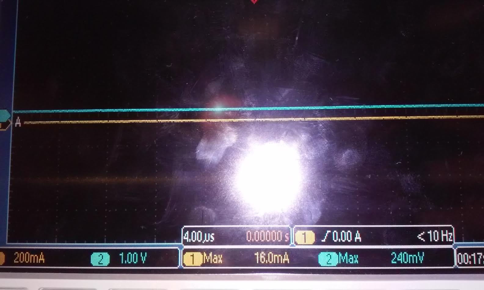
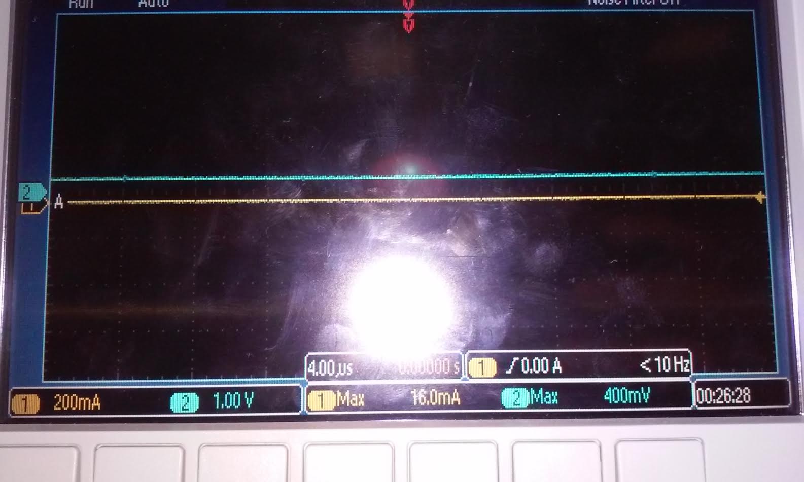
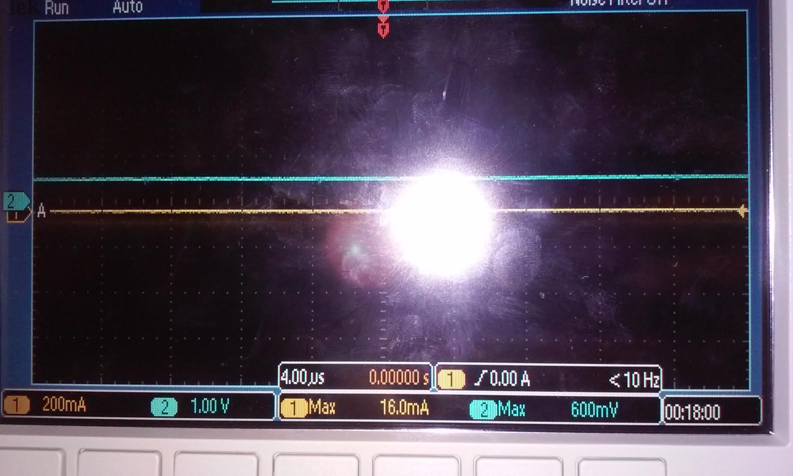
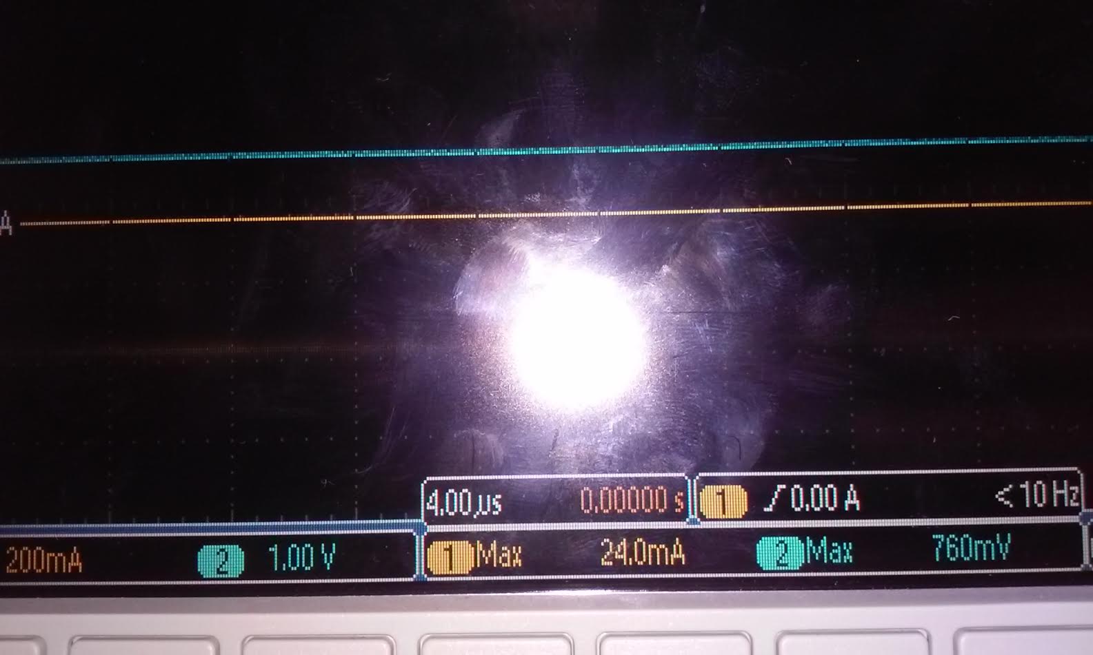
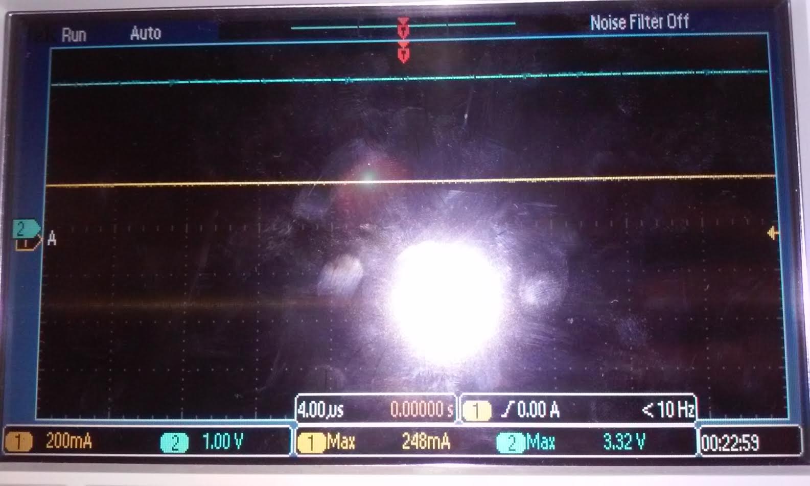
We
took picture of ID with VGS or VDS individually because we did not know
to to plot them on the scope. so we took data and use it to plot ID vs
VGS, ID vs VDS for both nmos and Pmos devices.
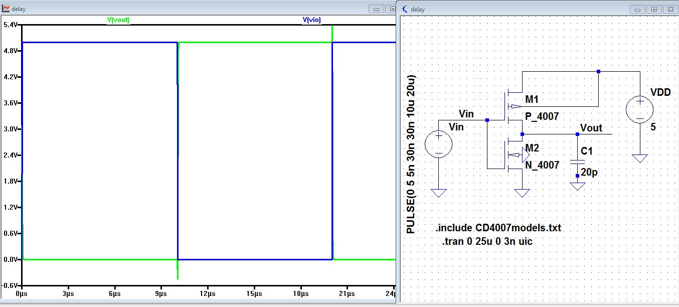
- Experimentally,
similar to what is seen on the datasheet (AC test circuits seen on page
3 of the datasheet), measure the delay of an inverter using these
devices (remember the loading of the scope probe is around 15 pF and
there is other stray capacitance, say another 10 pF).
time delay = 23.1 ns
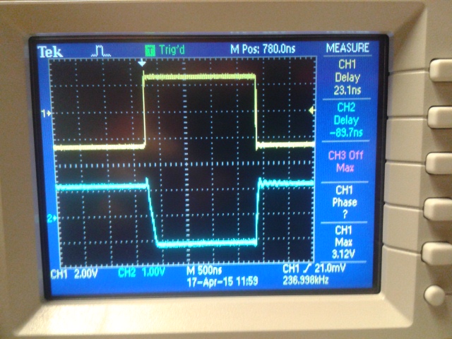
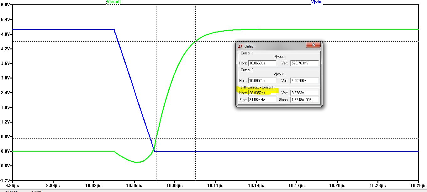
- Using
your model simulate the delay of the inverter and compare to measured
results. Adjust your SPICE model to get better matching between the
experimental data and the measured data.
Zoom-in of inverter plot: time delay = 28.9 ns
Return to EE420L front page